

Common mode impedance
What the choke presents to common mode noise, quoted at a stated frequency. Compare candidates at the same frequency or the numbers do not correspond.
インダクター製品
On a differential pair the choke has to suppress common mode noise without damaging the signal itself. Start from the interface and the frequency band your scan fails, then check that the impedance peak sits away from your signal's fundamental and that insertion loss stays acceptable.
型番検索・選定
この表では、海外サイトの現行製品データ、公開済みの選定項目、型番別の技術資料リンクを使用しています。
※画像列と型番列は固定されています。横にドラッグしてすべての仕様を確認できます
| 画像 | データシート | 比較 | ダウンロード |
サイズ
|
コモンモードインピーダンス(10MHz)最小値(Ω)
|
コモンモードインピーダンス代表値(Ω)
|
インダクタンス(uH)+50/–30%
|
最大RDC(Ω)
|
漏れインダクタンス(nH)代表値
|
最小絶縁抵抗(MΩ)
|
最大定格電流
|
最大定格電圧(V)
|
サンプル |
|---|
| 画像 | 型番 | データシート | 比較 | ダウンロード | サイズ | コモンモードインピーダンス(10MHz)最小値(Ω) | コモンモードインピーダンス代表値(Ω) | インダクタンス(uH)+50/–30% | 最大RDC(Ω) | 漏れインダクタンス(nH)代表値 | 最小絶縁抵抗(MΩ) | 最大定格電流 | 最大定格電圧(V) | サンプル |
|---|---|---|---|---|---|---|---|---|---|---|---|---|---|---|
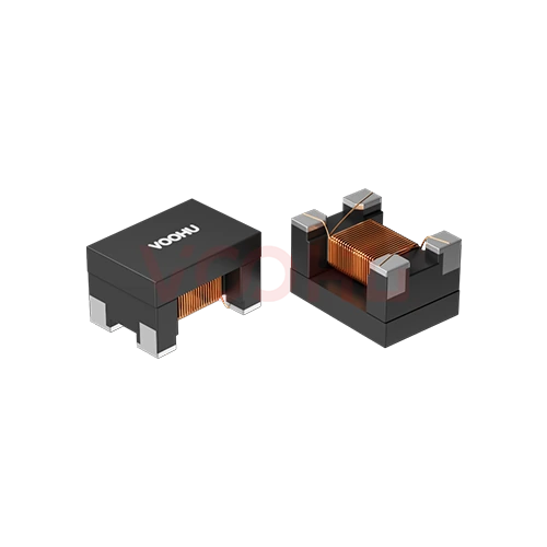 |
WHAC-4532A-110U0 | SPEC | 4532 | 300 | 600 | 11 | 1.2 | 50 | 10 | 250mA | 50 |
|
選択した条件を広げるか、現在の検索条件をクリアしてください。
By interface
The interface sets the data rate and therefore what the choke is allowed to do to the signal.
選定方法
Interface first, then the failing band, then signal integrity, then the footprint.
USB, CAN bus, Ethernet and HDMI each set a data rate and a signalling scheme. That determines how much the choke is allowed to affect the signal.
Read the frequency range where the radiated or conducted scan exceeds the limit, then look for a part whose impedance is high across that range.
Check the impedance peak does not sit near your signal's fundamental, and that DC resistance does not add unacceptable loss on the pair.
Measure the eye diagram and return loss on your own board. Datasheet curves are taken in a reference fixture, not in your layout.
Parameters
Impedance is quoted at a frequency; so is everything else that matters here.
What the choke presents to common mode noise, quoted at a stated frequency. Compare candidates at the same frequency or the numbers do not correspond.
Matters when the pair also carries bias or power, as on some bus and PoE-adjacent designs. On a pure signal pair it is rarely the binding constraint.
Adds loss in the signal path and causes a voltage drop where the pair carries current. Read the maximum figure rather than a typical value.
How much of the wanted signal the part removes. Low values matter more as the data rate rises; verify by measurement rather than by datasheet alone.
Sets the board area and the spacing available between the differential traces. Smaller packages ease layout but usually offer lower impedance.
Asymmetry between the two windings turns common mode into differential noise. It is the reason a choke can make an eye diagram worse rather than better.
比較
Package size and impedance level separate the families; the interface decides which fits.
選定表に戻る ↑| サイズ | 型番数 | コモンモードインピーダンス(10MHz)最小値(Ω) | コモンモードインピーダンス代表値(Ω) | インダクタンス(uH)+50/–30% | 最大RDC(Ω) | 漏れインダクタンス(nH)代表値 | 最小絶縁抵抗(MΩ) | 最大定格電流 | 最大定格電圧(V) | 操作 |
|---|---|---|---|---|---|---|---|---|---|---|
| 2012 | 13 | - | 120, 1200, 1000, 800, 380, 360, 260, 180, 90, 75 | - | 0.3, 0.35, 0.4, 0.45, 0.55, 0.88, 1.3, 1.5 | - | 10 | 280mA、300mA、400mA | 50, 125 | 絞り込み → |
| 3225 | 6 | 300, 500, 1000, 2200, - | 550, 1100, 2600, 5100, - | 11, 22, 51, 80, 100, 200 | 0.8, 1, 1.6, 2.5, 4, 4.9 | 50, 70, 130, 180, - | 10 | 70mA、150mA、200mA、250mA、300mA | 80 | 絞り込み → |
| 4532 | 21 | 300, 500, 1000, 2000, - | 600, 1200, 2800, 5800, 90±25%, 420±25%, 600±25%, 800±25%, 1000±25%, 1400±25%, 1400 | 11, 22, 51, 100, - | 0.25, 1.2, 1.4, 1.8, 2.5, 39, 60, 82, 89, 113, 148 | 50, 80, 150, 200, - | 10 | 150mA、200mA、250mA、700mA、1.0A、1.5A、1.8A、2.0A、2.2A、3.0A | 50 | 絞り込み → |
用途別確認
Confirm the interface, the data rate and whether the pair also carries bias current.
Documents
Datasheets carry the impedance curve, DC resistance and recommended land pattern.
代表的な入手可能資料を表示しています。特定のSKUは検索して確認してください。
VOOHUが公開する製品情報は、エンジニアリングチームが確認しています。仕様、ダウンロード資料、技術サポート情報は型番ごとに紐付けられているため、サンプルや見積もりを依頼する前に確認できます。
カテゴリー概要
On a power line the choke only has to pass current. On a signal pair it has to pass a waveform intact, which makes the selection harder.
型番が決まっている場合は、サンプルまたは見積もりを依頼。
A choke that works on a CAN bus can wreck a USB link, because the data rates differ by orders of magnitude. The interface sets how much insertion loss and how much impedance in the signal path the link can tolerate. Decide the interface and its rate before you start comparing impedance figures.
You want high common mode impedance across the band that fails your scan, and low impact at your signal's own frequencies. If the peak sits near the fundamental, the choke will attenuate the wanted signal as well as the noise. Read the curve, locate your two frequencies on it, and check they are far apart.
Real parts are never perfectly symmetric. Any imbalance between the two windings converts common mode noise into differential noise, which lands directly on the signal. This is why a choke sometimes makes an eye diagram worse. It cannot be predicted from the datasheet, so measure the eye and return loss on your own board.
よくあるご質問
Answers cover interface fit, eye diagram impact and how to compare candidates.
Because the interface sets the data rate, and the data rate decides how much the choke is allowed to affect the signal. A part that is fine on a CAN bus running at hundreds of kilobits can badly degrade a USB or HDMI link running orders of magnitude faster. Start from the interface, then filter on impedance.
Check where the impedance peak sits relative to your signal's fundamental frequency. You want the peak over the band that fails your emission scan and well away from the frequencies the signal occupies. Then check DC resistance and measure insertion loss on the real link.
Yes, and it is a common surprise. No real part is perfectly symmetric, and any imbalance between the windings converts common mode noise into differential noise that lands on the signal. That effect grows with data rate. The only reliable check is measuring the eye before and after on your own hardware.
Sometimes. A LAN transformer provides isolation and some common mode rejection, but on higher speed links or in difficult enclosures it may not be enough on its own. Whether an additional choke helps depends on your layout and your scan result, so measure rather than assume.
Only when the pair carries current as well as signal, which happens on some bus designs and in power-over-data arrangements. On a pure signal pair the binding constraints are impedance placement and insertion loss, not current. Read the datasheet for the specific case you have.
No. Package size tells you the footprint, not the electrical behaviour. Two parts of identical size can have very different impedance curves, DC resistance and symmetry. Compare the impedance at your frequency, the DC resistance and the recommended land pattern before treating one as a substitute.
Close to the connector, before the noise has a chance to couple into the rest of the board, and with the differential pair kept symmetric through the part. Asymmetric routing through or around the choke undoes much of its benefit, so treat the layout as part of the component choice.
With a complete part number, send the part number, quantity, delivery region and the date you need it. If you are still selecting, send the interface and data rate, the frequency band where your scan fails and the space available between the traces.
エンジニアサポート
候補型番と、確認が必要な条件をお送りください。候補が明確になった後にサンプル支援を追加でき、商取引に関するご質問も同じ技術相談の中でご相談いただけます。
資料のリビジョンも記載してください
温度、絶縁電圧、PoE電流の条件
ピン数、ピッチ、ピン列間隔
サンプルと評価の優先度確認に使用します
候補と相違点の比較が必要な時期
エンジニア確認により候補型番を選び、相違点をご説明します。
選定表またはエンジニア確認で選んだ型番
試作/パイロット生産/量産
サンプルと量産の時期を分けて記載してください
適合資料、材料宣言、第三者機関レポートなど
サンプル数量、リードタイム、費用は、プロジェクト段階と型番によって異なります。営業担当者より営業日にご回答します。