Ethernet Magnetics PCB Layout: Should There Be a Ground Plane Under the Magnetics?
Ethernet Magnetics PCB Layout: Should There Be a Ground Plane Under the Magnetics?
Not directly under the magnetics. In an Ethernet magnetics layout, keep a continuous ground plane under the MDI traces from the PHY to the transformer, then void it under the discrete transformer and the other parts on those traces. TI'sEthernet PHY PCB Design Layout Checklist (SNLA387)recommends a two-layer void for standard designs and an all-layer void for automotive ones, about 20 mil beyond the component edge, with no metal under the magnetics on any layer. The transformer then divides the port into a PHY side on logic ground and a cable side tied to chassis ground, with an isolation gap between them that no traces or planes cross. Keep chassis ground at least 20 mil from the rest of the board on all layers. VOOHU supplies discrete gigabit LAN transformers and RJ45 jacks with integrated magnetics, with layout data for the parts listed below.
Ethernet magnetics layout guidelines: four zones and one gap
Before routing, divide the area around the port into four zones. Length, impedance and matching rules for the MDI traces are in ourEthernet circuit design guide.
- PHY side.The PHY, its MDI pairs and the PHY-side center-tap connections, all over continuous logic ground.
- Magnetics.The discrete transformer over a ground void, with nothing else placed or routed under it.
- Cable side.The cable-side pins of the transformer, the center-tap termination and the RJ45 signal pins. This side returns to chassis ground through the termination, not to logic ground.
- Chassis ground.A copper area along the board edge for the RJ45 shield tabs and the enclosure contact, kept apart from logic ground on all layers.
The isolation gap runs across the board between zones 1 and 3, under the transformer body.
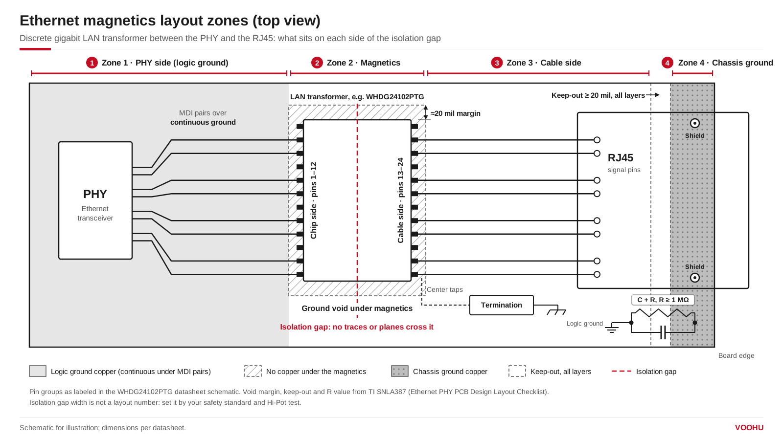
Layout zones around Ethernet magnetics. The chip-side and cable-side pin groups follow the WHDG24102PTG datasheet; the void margin and chassis keep-out follow TI SNLA387. Schematic for illustration; pin positions and dimensions per datasheet.
Which side of the transformer faces the PHY is set by the datasheet, not by the shape of the footprint. TheWHDG24102PTGdatasheet labels pins 1–12 as the chip side and pins 13–24 as the cable side, with each group on one long edge of the body. Place it with pins 1–12 toward the PHY, and the isolation gap falls between the two rows of pins, along the length of the body. If a schematic names the windings without marking a side, confirm the orientation with the supplier before you fix the placement.
Should there be a ground plane under Ethernet magnetics?
Not under the magnetics themselves. TI's checklist asks for continuous ground on the layer under the MDI traces, cut only under the components on those traces: the transformer or magnetics, chokes, AC coupling capacitors and ESD diodes. Standard designs get a two-layer void (the component layer and the layer below); automotive designs get an all-layer void, with two layers as the minimum. The void edge sits about 20 mil from the component edge in most designs, adjusted to your EMC requirements. No metal should be under the magnetics on any layer; if it cannot be avoided, a ground plane must at least separate it from them.
The reason is the job the transformer does. It isolates the cable from the equipment, and copper under its body adds capacitance between the two sides, which works against that isolation and gives noise a path around the windings.
How wide should the isolation gap be between the RJ45 side and the PHY side?
There is no single layout number for it. The gap has to support the isolation your product is rated and tested for, so its width comes from the safety standard your equipment is certified to and the Hi-Pot test it has to pass, not from a PHY layout checklist. The 20 mil figures in TI's checklist are the void margin and the keep-out around earth ground, not a creepage distance across the transformer. Whatever width you set, keep traces, vias and planes from crossing the gap on any layer. For how the barrier is tested, seewhy an Ethernet port fails the Hi-Pot test.
Ethernet chassis ground connection: where do the shield and termination go?
Connect the RJ45 shield tabs to the chassis ground zone. Keep chassis ground at least 20 mil from the rest of the board on all layers, and join it to logic ground only through a capacitor and a resistor of 1 MΩ or more, as TI recommends. The cable-side center taps go through the termination network to chassis ground; the resistor and capacitor values are covered in ourBob Smith termination guide. A product in a plastic enclosure has no metal chassis to return to, and the grounding plan changes; seeEthernet PCB design for plastic enclosures.
With an RJ45 jack that has integrated magnetics, part of that network is already inside the connector. In theSYT111Q066AA2A1D, the four cable-side center taps go through 75 Ω resistors to a 1000 pF, 2 kV capacitor that comes out on pin 10 (GND). In the PoESYT111Q334AB2A2DP057, each goes through 22 nF/100 V and 75 Ω to a 1000 pF, 2 kV capacitor tied to SHIELD, and the cable-side center taps are also brought out on pins P11–P14 (VC1–VC4). Route those pins as the datasheet shows.
RJ45 integrated magnetics PCB layout
A MagJack (RJ45 jack with integrated magnetics) moves the transformer and the termination into the connector, so the magnetics zone and the cable side sit inside one footprint. TI's checklist allows metal under an RJ45 connector with integrated magnetics, so the void rule for discrete magnetics does not carry over. Keep the PHY-side pairs over continuous ground up to the jack pins, keep chassis ground isolated around the shield pins, and follow the jack's own drawings. Where a separate common mode choke should sit relative to the transformer is covered incommon mode choke placement in Ethernet designs.
For the SYT111Q066AA2A1D, the datasheet gives a recommended PCB layout viewed from the component side: signal pins 1–10 in two rows at 1.27 mm pitch with 2.54 mm between rows, two locating posts, two shield pins and four LED pins (11–14). It also marks a keep-out area on the plug-in side of the footprint and a recommended panel cutout of 16.15 × 13.75 mm, for reference. Keep that area clear as drawn; for hole diameters, see the datasheet.
Ethernet magnetics layout checklist
| Check | What to do | Source |
|---|---|---|
| Ground under PHY-side MDI pairs | Continuous ground on the layer below; same-layer ground at least 3× the trace width away, 5× preferred | TI SNLA387 |
| Ground under discrete magnetics, chokes, AC coupling capacitors and ESD diodes | Void it: two layers (component layer and the layer below) for standard designs, all layers for automotive; void edge about 20 mil from the component edge | TI SNLA387 |
| Metal under discrete magnetics | None on any layer; if unavoidable, separate it by at least a ground plane | TI SNLA387 |
| Metal under an RJ45 with integrated magnetics | Allowed; follow the jack's keep-out area | TI SNLA387; jack datasheet |
| Transformer orientation | Chip-side pins toward the PHY, cable-side pins toward the RJ45, as labeled in the datasheet | Part datasheet |
| Isolation gap | No traces, vias or planes crossing it on any layer; width set by your safety standard and Hi-Pot test | Your product's safety standard |
| Chassis (earth) ground | At least 20 mil keep-out on all layers; joined to logic ground only through a capacitor and a resistor of 1 MΩ or more | TI SNLA387 |
| ESD protection | On the PHY side of the magnetics, per TI's Ethernet-specific ESD guidance | TI SNLA387 |
| Footprint | Use the datasheet's suggested pad or PCB layout and any keep-out area it marks | Part datasheet |
Which VOOHU magnetics come with layout data?
- WHDG24102PTG: gigabit 24-pin through-hole (DIP) LAN transformer, body 15.50 × 10.90 mm, rated −40 to +85 °C. The datasheet labels the chip side (pins 1–12) and cable side (pins 13–24) and gives a suggested pad layout, so the isolation gap is easy to place.
- WHSG24301TG: gigabit 24-pin surface-mount (SMD) LAN transformer with gull-wing leads, body 16.60 × 9.00 mm, 2.85 mm maximum height, suggested pads at 1.27 mm pitch, rated −40 to +85 °C. A PCB package file is on the product page; our FAE team can confirm which pin group faces the PHY for your layout.
- SYT111Q066AA2A1D: 1×1 gigabit RJ45 jack with integrated magnetics, tab down, with LEDs, rated −40 to +85 °C. The datasheet includes a recommended PCB layout, a keep-out area and a panel cutout, and the cable-side termination is built in.
- SYT111Q334AB2A2DP057: 1×1 gigabit PoE RJ45 jack with integrated magnetics, with the cable-side center taps brought out on pins P11–P14. A PCB package file is on the product page.
To compare more parts, use theLAN transformer selector filtered to 10/100/1000BASE-T, theRJ45 selector filtered to integrated magnetics, or browse our100/1000BASE-T LAN transformers.
产品WHDG24102PTG
产品SYT111Q066AA2A1D
方案/solution-ethernet/
FAQ
Q1: Should the RJ45 shield connect to chassis ground or signal ground?
Chassis ground. Tie the shield tabs to the chassis ground zone at the board edge, and connect chassis ground to signal (logic) ground only through a capacitor and a resistor of 1 MΩ or more, as TI's layout checklist recommends. Keep at least 20 mil of keep-out between the two grounds on all layers.
Q2: Can I route traces under Ethernet magnetics?
Not on any layer, according to TI's checklist. If a signal has to pass under the magnetics, it must be separated from them by at least a ground plane. Route around the transformer instead and keep the void under it clear.
Q3: Where should ESD protection go relative to the magnetics?
On the PHY side. TI's layout checklist points to its Ethernet-specific ESD guidance, which places the protection device on the PHY side of the magnetics because the connector side can see high common-mode voltage swings. Check that the device's working range suits the signal voltages in your PHY datasheet.
Have your Ethernet port layout checked
Laying out a new Ethernet port? Send the port area of your layout, the PHY and the magnetics you plan to use through oursample and support form. Our FAE team can check the transformer orientation, the pin assignment and the footprint against the datasheet, and suggest suitable LAN transformers or RJ45 jacks with integrated magnetics. Samples are available for evaluation, and selected parts are free of charge. Our FAE team will be glad to confirm the options for your project. VOOHU supplies RJ45 and SFP connectors, LAN and PoE transformers and common mode chokes from Suzhou, China, to more than 1,500 customers.
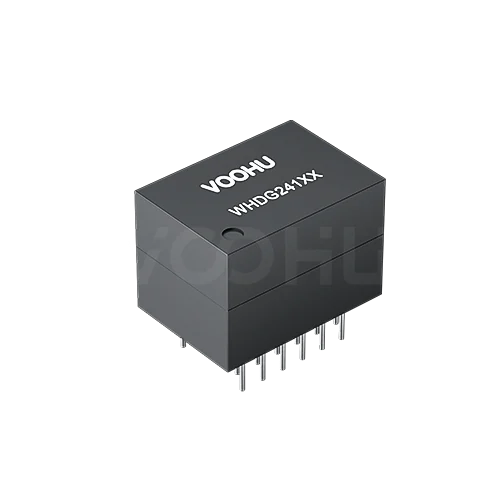 WHDG24102PTG Single Port DIP Gigabit Base-T PIN24 PoE 720mA LAN Transformer
> View Details
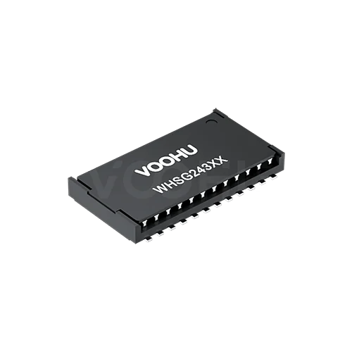 WHSG24301TG Single Port SMD(Low height)Gigabit Base-T PIN24 non-PoE LAN Transformer
> View Details
 SYT111Q334AB2A2DP057 90° side insertion 1*1 Tab Down POE 600mA G/Y 100/1000M DIP RJ45
> View Details
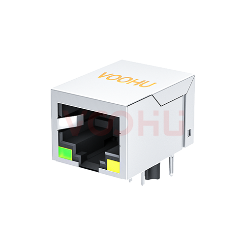 SYT111Q066AA2A1D 90° 1*1 Tab Down LED G/Y 100/1000BASE DIP RJ45
> View Details