
【Product Selection Guide】 Reintroducing VOOHU Electronics SFP Connectors—Far More Than Just a "Cage for Optical Modules"
【Product Selection Guide】 Reintroducing VOOHU Electronics SFP Connectors—Far More Than Just a "Cage for Optical Modules"
In today’s rapidly advancing world of high-speed data communication and optical interconnect technology, SFP cages have become indispensable physical interfaces in network equipment. From Gigabit to 800G, from data centers to 5G front‑haul, the form factors of SFP, SFP+, SFP28, QSFP, QSFP‑DD continue to evolve. However, many engineers still hold misconceptions about their selection, compatibility, EMI design, and PCB layout.
VOOHU Electronics (VOOHU) has been deeply involved in SFP/SFP+/SFP28/QSFP series cages for many years, providing a full range of cages and integrated connectors from 1×1 to 2×N, supporting press‑fit, soldering, SMT and other mounting methods, and offering options such as light pipes, heat sinks, and EMI fingers. These products meet complete interconnect needs from Gigabit to 400G/800G. All products are signal‑integrity verified, and reference layouts and simulation support are available.
Re‑understanding the SFP Cage
Many engineers’ first reaction to an SFP cage is “it’s just a metal shell to hold an optical module.”
But after encountering the following situations, you realise it is not that simple.
-
1.System EMC test – radiated emissions exceed the limit at 6GHz. After investigation, the cause is a gap between the SFP cage and the front panel, leading to EMC certification failure.
-
2.25G optical module suffers frequent bit errors – after trying several modules, the root cause is that the high‑speed differential vias on the PCB were not back‑drilled; the via stubs introduce high‑frequency reflections, and the signal eye diagram completely collapses.
The SFP cage is not a passive “enclosure”, but a system‑level component that carries three engineering responsibilities. Failure in any one of them costs far more than the price of the cage itself.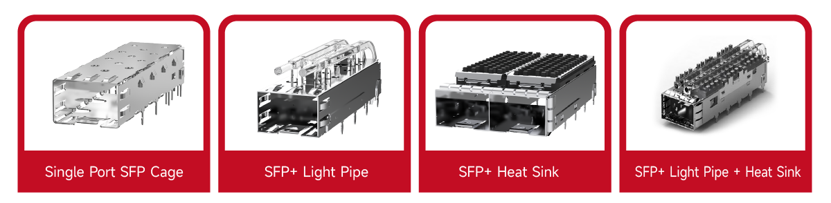
The SFP cage performs three core responsibilities in a system, each directly affecting overall performance and reliability.
-
EMI shielding – The cage encloses electromagnetic radiation generated by high‑speed signals, preventing leakage. Shielding failure can cause EMC non‑compliance, severe interference to adjacent channels, leading to bit errors or packet loss.
-
Mechanical retention – The cage provides a stable plug/unplug structure for the module at the panel opening, ensuring contact reliability over long‑term use. Unreliable retention leads to loose insertion, intermittent contact under vibration, eventually causing transient link interruption or complete failure. -
Thermal management – The module generates heat during operation; the cage must effectively conduct that heat to the system airflow path. Inadequate thermal design causes the module to throttle down due to overheating, or even suffer permanent damage.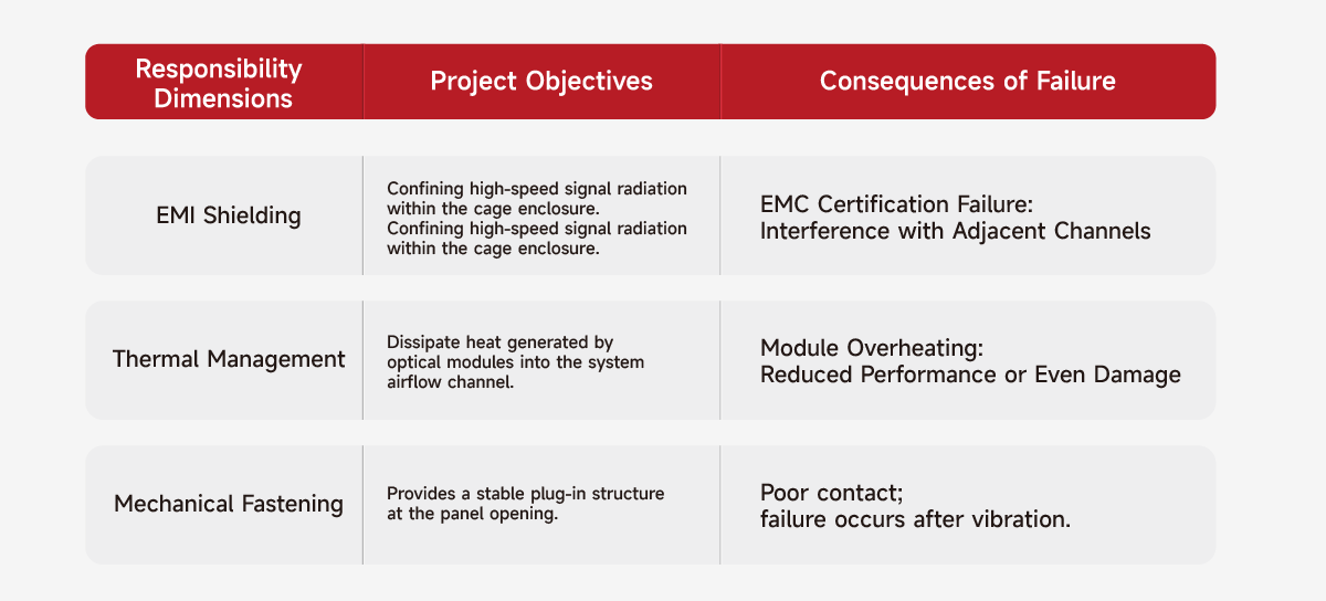
Why do SFP+ and SFP use the same interface?
Since its definition in the early 2000s, the SFP family has increased speed from 1G to 25G, spawning nearly ten sub‑families. Looking only at datasheets, these families may seem irregular, but the underlying logic always follows two principles: compatibility and power consumption.
Compatibility: interface unchanged, speed doubled
If every speed upgrade required a new cage interface, the whole chassis, PCB and enclosure would be redesigned, instantly nullifying investment in existing equipment. Over three generations – SFP → SFP+ → SFP28 – speeds jumped from 1G to 10G to 25G, yet the cage kept the same 20‑pin mechanical structure. This means: an SFP28 port can downwards‑accept SFP+ and SFP optical modules, running at reduced speed. Users upgrade network speed by only changing the optical modules, not the switch. “Keeping the 20 pin” trades minimal hardware change for maximal rate iteration.
Power consumption: if a single lane cannot go faster, add lanes; if lanes cannot be added, change the package
When single‑lane speed approaches the physical limit, engineers add lanes, increasing interconnect density.
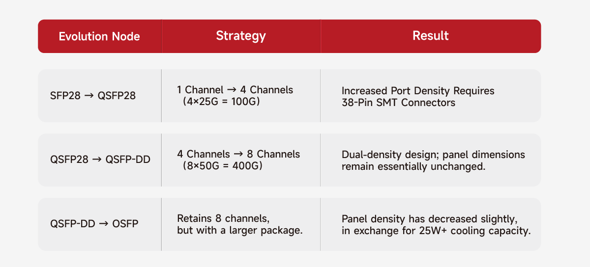
The evolution of SFP cages is essentially a trade‑off between lane count and package:
-
From SFP28 to QSFP28: single lane expanded to 4 lanes to reach 100G, at the cost of changing the cage from 20‑pin through‑hole to 38‑pin SMT.
-
From QSFP28 to QSFP‑DD: 4 lanes doubled to 8 lanes to achieve 400G, using a double‑density design; panel size unchanged but crosstalk becomes more sensitive.
-
OSFP, while keeping 8 lanes, enlarges the package. It sacrifices some panel density but gains heat dissipation capability above 25W, adapting to the high power demands of AI clusters.
Quick Reference Table of Key Parameters for the Full Series
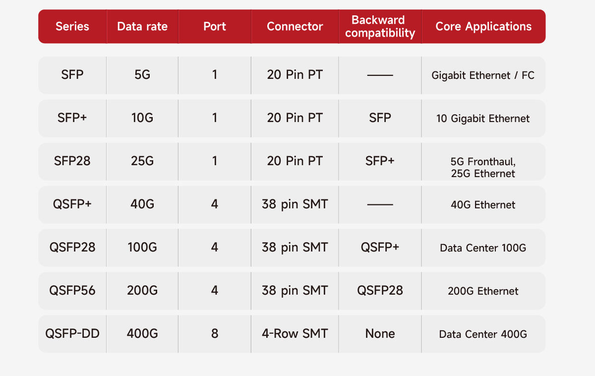
High‑rate cages are downwards compatible with lower‑rate modules, but low‑rate cages must never accept high‑rate modules – “fits ≠ works”, signal integrity cannot be guaranteed.
From 1G to 800G, the evolution roadmap of the SFP family is clear:
-
SFP supports 1G/4.25G, uses a 20‑pin through‑hole cage, for Gigabit Ethernet.
-
SFP+ increases to 10G, downwards compatible with SFP, becomes the mainstay for 10G.
-
SFP28 retains the 20‑pin through‑hole, reaches 25G, compatible with the previous two generations, widely used for 5G front‑haul.
-
When single‑lane speed approaches the limit, multi‑lane schemes become mainstream:
-
QSFP+ achieves 40G via 4 lanes, using a 38‑pin SMT cage.
-
QSFP28 downwards compatible with QSFP+, achieves 100G via 4×25G, dominates data centers.
-
QSFP56 further increases 4 lanes to 200G.
-
-
For higher density:
-
QSFP‑DD uses 8 lanes with a dual‑row SMT design; panel size unchanged, compatible with QSFP28, achieving 400G.
-
OSFP uses a dedicated interface, sacrificing some panel density in exchange for heat dissipation above 25W, designed for the 800G needs of AI clusters.
-
VOOHU Electronics covers all the above rates and packages, offering multi‑port combinations from 1×1 to 2×N, supporting industrial‑grade wide temperature and custom options such as heat sinks and light pipes.
Three Selection Questions: Nailing Down the Correct Model
At the selection stage, engineers can quickly determine the candidate range by answering just these three questions.
Question 1: How fast do you need to go?
-
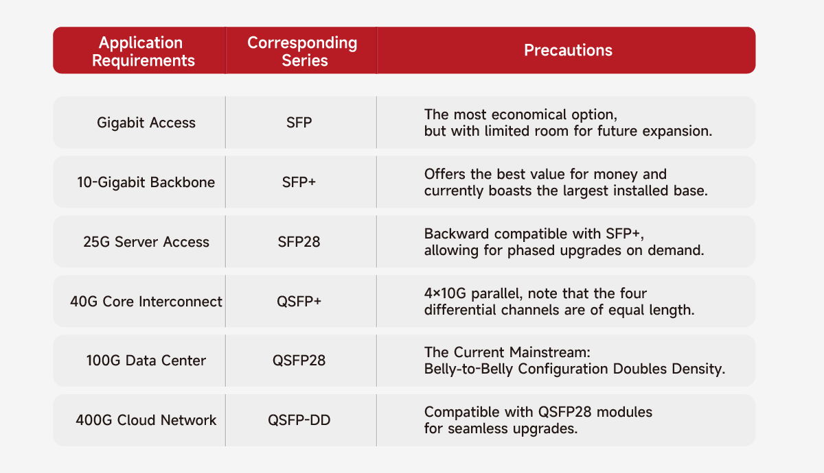
Gigabit access scenario: the most economical choice is SFP, but future expansion is limited; suitable for cost‑sensitive projects with fixed speed requirements.
-
10G backbone – recommended SFP+: best price/performance, currently the largest deployed volume in existing networks, the main choice for 10G access.
-
25G server access – SFP28: downwards compatible with SFP+, allows stepwise upgrade, balancing present and future.
-
40G core interconnect – QSFP+: internally 4×10G parallel; special attention must be paid to length matching of the four differential pairs.
-
100G data center – currently mainstream QSFP28: supports belly‑to‑belly mounting, doubling port density within limited panel space.
-
400G cloud network – QSFP‑DD: downwards compatible with QSFP28 modules, supports smooth upgrade from 100G to 400G.
Question 2: How many ports do you need?
-
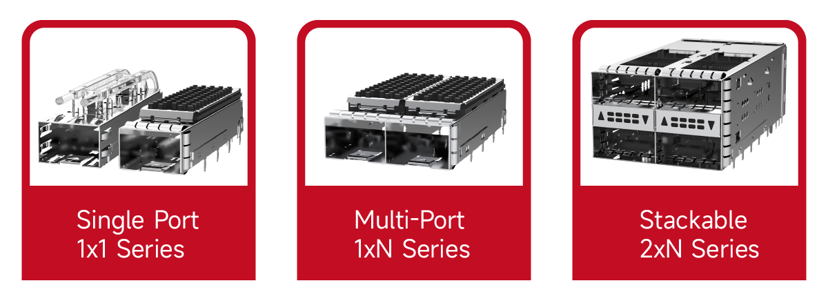
Few ports (1‑4): use 1×1 or 1×N single cages; flexible layout, simple thermal design, suitable for low‑density scenarios.
-
4‑12 ports: 1×N ganged cages are recommended. Pay attention to EMI coupling between adjacent ports, and reserve enough space for finger compression to ensure grounding reliability.
-
12‑48 ports: 2×N stacked cages are a better choice. They save about 50% of PCB area, but crosstalk between upper and lower rows and heat accumulation are more pronounced; dedicated simulation is required during design to ensure signal integrity and airflow.
-
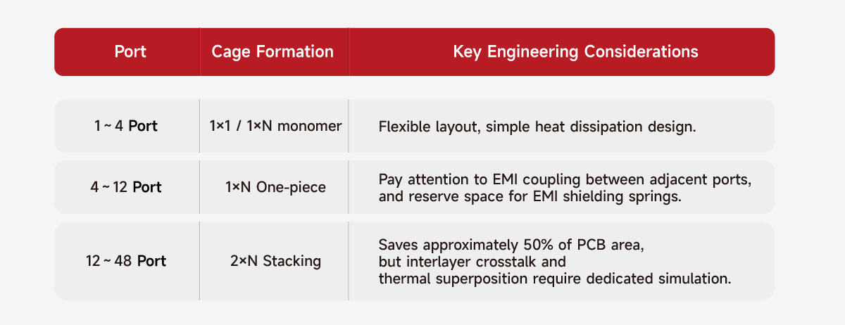
Special note: although 2×N stacking saves area, the thermal structure of the upper ports blocks airflow to the lower row, and crosstalk between high‑speed differential pairs of upper and lower rows is easier to occur. For each additional stacking layer, the workload of EMI and thermal simulation increases by an order of magnitude; evaluate fully before selection.
Question 3: In what environment will it operate?
-
High‑density data centre (above 40°C): heat dissipation is the primary concern. An SFP cage with an external heatsink is mandatory, and the heatsink height must match the chassis airflow direction to ensure effective heat extraction.
-
Outdoor or industrial environments (humidity, salt spray): material choice is critical. Stainless steel base with nickel plating is recommended; bare copper alloy oxidises easily in such conditions, leading to poor grounding and mechanical strength degradation.
-
Strict EMC requirements (e.g., medical, military equipment): enhanced EMI shielding design: dual protection with EMI fingers and conductive gaskets; additionally, copper pour and solder on the PCB under the cage to create a low‑impedance ground path.
-
Cost‑sensitive SME applications: on the premise of maintaining reliability, optimise configuration – use stainless steel base to reduce cost; light pipes installed only if required; use ventilation holes instead of external heatsinks to balance performance and budget.
EMI Shielding
In high‑speed communication systems, electromagnetic interference (EMI) is a key challenge affecting signal integrity and equipment stability. The EMI shielding performance of an SFP cage directly determines whether the system passes EMC certification.
-
First line of defence: cage finger sealing. Metal fingers are designed around the SFP cage; when assembled, they make reliable contact with the chassis panel, forming a continuous low‑impedance path to ground.
-
Second line of defence: the metal shell of the cage is a critical EMI shield. Only by connecting it to the PCB’s chassis ground with large area and low impedance can an effective Faraday cage be formed, directing electromagnetic radiation to earth and preventing signal leakage.
PCB Design and Signal Integrity
Pad impedance discontinuity – the hard requirement of 100Ω ±10% for differential pairs
There is usually a large reference plane directly under the SFP pads, causing a sharp impedance drop at that point. Two recommended approaches: (1) hollow out the reference plane directly under the pads to compensate for the impedance drop; (2) use a gradual line width transition to avoid abrupt impedance change. Target: 100Ω ±10%.
AC coupling capacitors – place close to pins, keep symmetry
Most SFP interfaces require 100nF AC coupling capacitors in series on the transmit and receive differential lines. They block the DC component, preventing the optical module’s internal DC bias from affecting the host‑side circuit. Layout requirement: capacitors should be placed as close as possible to the SFP pins, and the positions of the capacitors on the two differential lines must be symmetrical to maintain differential pair timing consistency.
Via stub – back drilling is mandatory
SFP pins are often through‑hole structures. In multi‑layer PCBs, a via penetrates multiple layers; the unused copper portion (“stub”) below the signal layer introduces reflections at high frequencies, causing eye diagram degradation or even complete collapse. For high‑speed signals at 10G and above, back drilling must be performed on the signal vias to remove the unused copper stub and eliminate stub reflections.