


Chiplan and network transformer selection
Chiplan and network transformer selection
The following is a more comprehensive technical comparison and design analysis of capacitive/inductive Chip LAN and integrated network transformers. The content is about 2 times deeper than the initial version, adding device internal structure analysis, more practical design challenge descriptions and industry application technology cases:
────────────────────────────────────────────────
Part 1: Capacitive Chip LAN vs Integrated Network Transformer - A Systematic Analysis from Principle to Implementation
1. Device structure and physical principle
Capacitive Chip LAN:
- Architecture decomposition:
- Internally integrated high-voltage ceramic capacitors (withstand voltage 1-2kV) serve as an isolation layer, with differential-mode signal transmission networks connected on both sides.
- Comes with ESD protection diodes and micro common mode inductors to suppress spikes and EMI.
- Typical package: 0402/0603 chip package, full SMD design, no magnetic core.
- Signal path model:
- Presents low impedance to high frequencies, allowing signals to pass, but the DC path is blocked by the capacitor.
- Parasitic inductance (about 1-2nH) and distributed capacitance (0.5-1pF) directly affect the attenuation of signals above 10G.
Integrated network transformer:
- Architecture decomposition:
- Magnetic isolation core: Ferrite magnetic toroid or planar transformer structure, primary to secondary winding ratio 1:1 (or customized).
- Peripheral circuit: Built-in Chip RC network to balance common mode impedance, some modules integrate common mode choke (CMC).
- Package: DIP/SMD module (size 6x6mm to 15x15mm) with metal shielding.
- Magnetic coupling efficiency:
- The initial permeability (μi) and saturation flux density (Bs) of the core material determine the bandwidth and power handling capability.
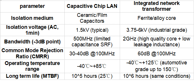
Key parameter comparison: capacitor type vs transformer type
────────────────────────────────────────────────
2. Deep challenges and solutions for hardware design
(1) Capacitive Chip LAN Design Risks
- Capacitor withstand voltage degradation:
- Repeated charging and discharging of high frequency and high voltage (such as PoE applications) causes aging of the capacitor dielectric and increased leakage current.
- Countermeasure: Choose high-stability ceramic capacitors such as X7R/X8R, and reserve 20% voltage margin.
- High frequency loss control:
- When the signal frequency is >1GHz, the capacitor self-resonant frequency (SRF) limits the effective bandwidth.
- Countermeasures: Shorten the trace length from PHY to capacitor (<5mm), disable vias and right-angle turns.
(2) Design risks of integrated network transformer
- Magnetic saturation problem:
- In high-power scenarios such as PoE++ (90W), large currents cause core saturation and skyrocketing losses.
- Countermeasures: Choose Sendust or nanocrystalline cores with high Bs values and increase the air gap (sacrificial inductance).
- High frequency radiation interference:
- Unshielded transformers become radiation sources in the GHz band, affecting RF circuits (such as Wi-Fi/BT modules).
- Countermeasures: Ground the module housing and arrange magnetic absorption materials (such as ferrite sheets) around it.
────────────────────────────────────────────────
3. Application scenario technology adaptation and typical cases
(1) Flexible application of capacitive chip LAN
- Fast charging and data transmission two-in-one (USB PD + Ethernet):
- In a USB Type-C docking station, use capacitive LAN to save space while supporting 100W power delivery.
- Design difficulty: PD protocol communication (CC line) and differential signal must be strictly isolated to prevent capacitive coupling noise.
- Industrial IoT low-power sensor network:
- In the RS-485 to Ethernet gateway, the capacitor isolation meets the basic 2kV withstand voltage, and there is no core hysteresis at -40℃ low temperature startup.
(2) High-end applications of integrated transformers
- 800G optical module SerDes interface isolation:
- Use ultra-wideband (supporting 56G PAM4) transformers and combine them with Linear Drivers to compensate for losses.
- SI verification: Use TDR (time domain reflectometer) to ensure impedance matching and PCB routing error within ±5%.
- Gigabit Ethernet backbone for electric vehicles:
- Mechanical reinforcement design of core and coil, epoxy resin potting to prevent breakage under vibration and temperature shock.
────────────────────────────────────────────────
Part 2: Inductive Chip LAN vs Integrated Network Transformer - Breakthrough in High Frequency Performance and Reliability
1. Technological innovation of inductive chip LAN
(1) Fusion of magnetic integration and semiconductor technology
- 3D stacked inductor technology:
- Use TSV (through silicon via) to manufacture spiral inductors on silicon substrates, increasing the Q value by 30% and supporting 10GHz ultra-wideband.
- Typical manufacturers: TDK’s MLP series (Multi-Layer Pieced Inductor).
- Magnetic and electric composite isolation:
- Inductive isolation + capacitive coupling dual path, redundant design improves EMC level (such as meeting CISPR 32 Class B).
(2) Performance limits of inductive vs. traditional transformers

────────────────────────────────────────────────
2. High-frequency traps and cracking methods in hardware design
(1) Signal ringing suppression for inductive chip LAN
- Root cause:
- High-speed signal edges (<100ps) trigger LC resonance, and ringing causes the bit error rate (BER) to increase.
- Countermeasures:
- Add a 22Ω resistor (or an adjustable termination network) in series on the PHY side to match the driver impedance.
- PCB stack-up optimization: reference plane is complete (avoid cross-segmentation), and the spacing between signal layer and GND layer is <4mil.
(2) Multi-port crosstalk control of integrated transformer
- Root cause:
- Magnetic field coupling of multi-port transformers in switches deteriorates far-end crosstalk (FEXT).
- Countermeasures:
- The module spacing is ≥10mm, and a shielded ground plane is inserted between signal layers (Stripline structure).
- Serial ports are arranged in staggered layout, breaking the symmetrical coupling.
────────────────────────────────────────────────
3. Industry cutting-edge applications and technology trends
(1) SiP integration of inductive chip LAN
- Heterogeneous integration cases:
- Intel “Ethernet SiP”: PHY chip, inductor isolation, and TVS are integrated in a 5x5mm package with a rate of 2.5Gbps.
- Advantages: Reduce PCB area by 60% and increase yield to 99.8% (traditional modules 97%).
(2) Magneto-optical hybrid isolation technology
- Technical route:
- VCSEL (Vertical Cavity Surface Laser) and photodiode are embedded in the transformer magnetic circuit to achieve electric-magnetic-optical triple isolation.
- Withstands voltage exceeding 30kV and has been used in UHV substation monitoring systems.
(3) Research and development of quantum dot magnetic cores
- Innovation:
- Quantum dot-doped magnetic materials reduce high-frequency losses by 50%, supporting 1THz terahertz communication prototypes.
- Potential scenarios: 6G wireless backhaul network, high-precision radar interference isolation.
────────────────────────────────────────────────
4. Engineer Selection Decision Tree
Step 1: Prioritize requirements
- Isolation withstand voltage > 3kV? → Select a transformer
- Space cost sensitive? → Choose capacitive
- Rate > 10Gbps? → Choose transformer or advanced inductor
- Need automotive-grade certification? → Choose AEC-Q200 transformer
Step 2: Verify supply chain stability
- Capacitive Chip LAN: The supply cycle of Taiwanese manufacturers (Yageo/Walsin) is 8 weeks, and the yield of domestic alternatives (Fenghua) needs to be improved.
- Integrated transformer: Japan's TDK/Murata has a delivery time of 12 weeks, and the domestic alternative Magnetron Technology needs to evaluate long-term reliability.
Step 3: Preliminary research and test project
- Required items: Isolation withstand voltage test, TDR impedance verification, Thermal cycle (-55℃~+125℃ 1000 times)
- Optional items: HBM ESD test, salt spray corrosion test (maritime equipment), random vibration analysis (vehicle-mounted).
────────────────────────────────────────────────
Summarize
Capacitive/inductive Chip LAN and integrated network transformer each have their own technical advantages:
- Miniaturization and cost: Capacitor/inductor Chip LAN dominates consumer electronics and lightweight IoT.
- Extreme reliability and performance: Integrated transformers are still the best choice for industrial, automotive and military applications.
- Future battlefield: 3D magnetic integration, quantum magnetic core, and magneto-optical hybrid isolation technology will reshape the industry landscape.
Design motto: "Isolation level and signal integrity are the first principles, and everything else is a trade-off."

Newsletter subscription
Subscribe to our newsletter and stay updated on the latest information of our company and product.
Name
|
I agree that the information that I provide will be used in accordance with the terms of Voohu International Inc. Privacy & Cookies Policy


