


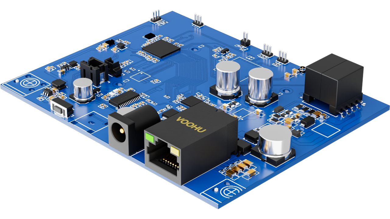
ETH's PCB Design Strategy for Plastic Housing
Analysis of ESD Protection Characteristics of Plastic Enclosures
Plastic enclosures are essentially an isolation strategy. According to ESD protection principles, isolation is the most direct and effective protection method—by increasing the discharge path length, static electricity cannot reach the internal circuitry. The IEC 61000-4-2 standard stipulates that an 8kV air discharge requires at least 4mm of insulation distance to effectively prevent arc penetration. This provides a theoretical basis for plastic enclosure design: as long as sufficient air gaps and creepage distances are maintained, the plastic enclosure itself is a natural barrier. However, this isolation characteristic also brings side effects: static charges generated inside the device or externally coupled charges cannot be discharged smoothly, potentially forming a high-voltage potential in a certain area of the PCB. When the voltage accumulates to a level sufficient to break down the plastic enclosure or air gap, a more destructive secondary discharge will occur. Therefore, the core of charge management under plastic enclosures lies in "active discharge" rather than "passive isolation."
- Charge Dynamics of Floating Ground Systems
Plastic-cased devices typically constitute floating ground systems, meaning there is no DC connection between the PCB ground plane and the external ground. The charge behavior of floating ground systems follows these principles:
Charge Conservation: The total amount of positive and negative charges within the system is equal, but different areas may exhibit different potentials due to induction.
Capacitive Coupling: Parasitic capacitances form between the PCB and the external environment, and between internal components and the casing, becoming channels for charge transfer.
High Voltage Accumulation: In the absence of a discharge path, a small charge can generate thousands of volts at high-impedance nodes.
Discharge Threshold: When the potential difference exceeds the breakdown strength of the insulating medium, an arc discharge occurs.
Core Design Principles for PCB-Level Charge Discharge
Principle 1: Construct a Board-Level Quasi-Ground Plane
In plastic-cased devices, although an external ground connection is not possible, a stable reference potential plane must be established on the PCB, which we call "quasi-ground." This plane serves as a "reservoir" and "transfer station" for charge.
Design considerations include:
- Complete Ground Plane: When using multilayer board designs, ensure there is a complete, unsegmented copper foil layer as a continuous ground plane. A complete plane provides the lowest impedance path and quickly homogenizes charge distribution.
- Star Grounding Topology: Connect the ground wires of all functional modules to the main ground plane in a star configuration to avoid potential differences caused by ground loops.
- Avoid Ground Segmentation: Do not functionally segment the ground plane. Segmentation leads to inconsistent ground potentials in different areas at high frequencies, creating potential differences.
- Maximize Copper Filling: Fill all unused PCB areas with copper foil and connect them to ground to increase charge capacity.
Principle 2: Establish a Hierarchical Discharge Network
To prevent excessive charge concentration at a single node, a hierarchical discharge network should be designed to achieve gradual charge release. This network is similar to the tiered flood discharge system of a dam:
Level 1: Board-Level Homogenization Layer
- Design a ring-shaped ground plane with a width of at least 3.5mm around the PCB as a charge "buffer".
- Connect the ring-shaped ground plane to the main ground plane through dense vias (5mm spacing) to reduce connection impedance.
- The protection ring around critical ICs should be directly connected to this ring-shaped ground plane.
Level 2: Interface Discharge Protection
- All external interfaces (RJ45, USB, power, etc.) must have independent ESD protection devices.
- The ground terminal of the protection device should be connected to the main ground plane through the shortest path (<5mm).
- Avoid sharing ground planes between protection devices and protected circuits to prevent ground bounce.
Level 3: Energy Dissipation Layer
- Set up "charge dissipation zones" at the four corners or edges of the PCB—connect large areas of copper foil to the main ground through an RC network.
- RC parameter selection: A 1MΩ/10MΩ resistor and a 10nF/100nF capacitor are connected in parallel to form a high-frequency, low-impedance, high-DC-impedance discharge path.
- This design allows for rapid high-frequency electrostatic discharge while blocking DC leakage current and maintaining floating ground characteristics.
Principle 3: Optimize Layout for Spatial Isolation
The spatial layout under the plastic casing directly affects charge distribution and discharge efficiency. A "concentric circle" layout concept should be followed:
ESD Source Identification and Isolation
- ESD test points are typically located at enclosure seams, ventilation holes, operation buttons, indicator lights, etc.
- During PCB layout, designate the corresponding areas of these sensitive locations as "no-go zones," where no components or traces should be placed.
- Ensure that the creepage distance between the ESD source and internal circuitry is greater than 20mm; this is crucial to preventing secondary arcing.
Functional Zoning Strategy
- Place sensitive components such as Ethernet PHY chips and transformers in the center of the PCB.
- Place robust circuits such as power supplies and interface drivers on the periphery of the PCB.
- Create a "protective strip" between sensitive areas and edges—a blank area of at least 3mm or an isolation strip consisting only of ground wires.
Handling Highly Sensitive Signals
- Sensitive traces such as reset, clock, and analog front-end signals should be routed on inner layers of the PCB and surrounded by ground planes on both sides.
- These signal lines should be kept at least three times the trace width away from the board edge.
- Avoid placing vias near sensitive signals to prevent charge coupling through vias.
Principle 4: Controlled Impedance Discharge Path
In plastic-cased devices, a purely floating ground is not ideal; a controlled impedance discharge path needs to be constructed. This path must ensure effective ESD energy release while maintaining the device's floating ground characteristics to suppress power frequency interference.
RC Discharge Network Design
According to the IEC 61000-4-2 standard, ESD testing requires a 2kV discharge within 10 seconds for each discharge. Therefore, the discharge resistance value can be calculated as: R = V/I = 2000V / (Q/t) ≈ 1MΩ/2MΩ.
Recommended for practical design:
- Resistors: 1MΩ/10MΩ, withstand voltage at least 2kV
- Capacitors: 10nF/100nF, withstand voltage above 1kV, preferably X7R or C0G material
- Layout: The RC network should be close to the PCB edge, especially in areas where human contact is possible.
Component Peripheral Design Principles
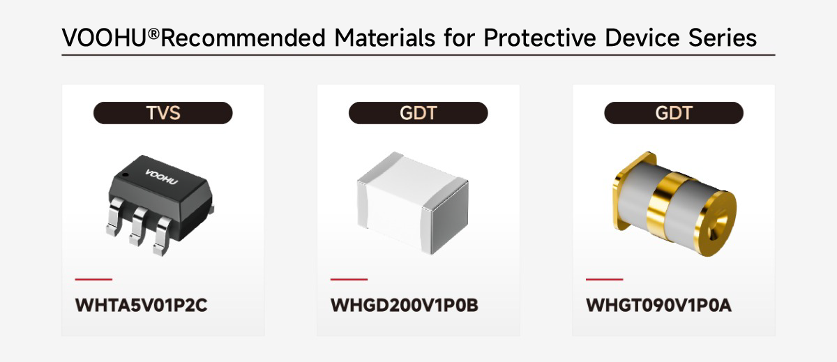
The Synergistic Effect of TVS and GDT
- At critical interfaces, TVS (Transient Voltage Suppressor) provides a fast-response path, clamping ESD energy.
- For high-voltage ESD, GDT (Gas Discharge Tube) can be connected in parallel to provide a large energy discharge path.
- The grounding terminals of both TVS and GDT must be connected to the main ground plane via independent, short, and wide traces.
Network Transformer Shielding
Ethernet transformers are crucial barriers against ESD conduction, and their design quality directly impacts protection effectiveness:
- Choose transformers with center taps and ground the taps via capacitors.
- The primary and secondary ground planes of the transformer should be separated, coupled only through capacitive coupling.
- Do not route cabling under the transformer; maintain a complete ground plane as shielding.
MDI Signal Line Protection
Physical Layer Medium Dependent Interface (MDI) traces are the entry point for ESD:
- Place an ESD protection array (such as the SP03xx series) before the MDI pins of the PHY chip.
- The ground pin of the protection device should be directly connected to the main ground plane via a dedicated via.
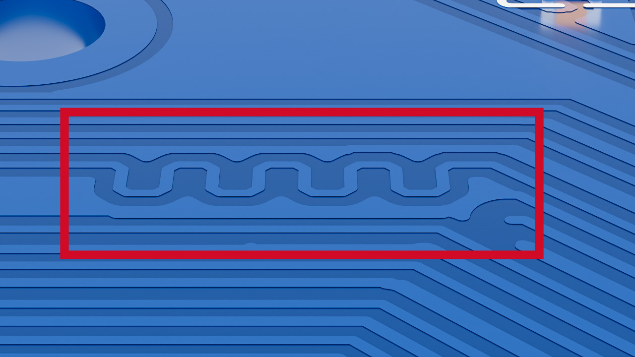
- MDI traces should be as short as possible, ideally under 25mm, and impedance matched to 50Ω.
- Surround the traces with a ground plane, and densely insert vias on both sides to form a "shielding wall."

Newsletter subscription
Subscribe to our newsletter and stay updated on the latest information of our company and product.
Name
|
I agree that the information that I provide will be used in accordance with the terms of Voohu International Inc. Privacy & Cookies Policy


