
VOOHU Chip LAN chip network transformer selection: PHY matching, PoE bias and reflow soldering verification
VOOHU Chip LAN chip network transformer selection: PHY matching, PoE bias and reflow soldering verification
Chip LAN chip network transformers are often found in the most crowded interface areas on wireless access points, industrial gateways, network cameras and small switches. Just because the prototype can start up normally at room temperature does not mean that the mass-produced board is necessarily stable: after reflow soldering, increased PoE load, or the entire machine entering a high-temperature environment, individual ports may be renegotiated, bit errors may increase, or EMC results may drift. At this time, only the package length and width are compared, and the real boundary is often not found. What functions the device performs in the circuit, what type of PHY topology it cooperates with, how the DC bias passes through the magnetic components, and whether the pad and reflow process are controlled must be placed in the same verification list.
Among the Chip LAN products on the VOOHU official website, there are both X'fmr+CMC combinations and Cap+CMC combinations; they belong to the same product series, which does not mean that they can be directly interchanged at the same schematic position. This article selects four accessible public part numbers as reference for preliminary selection, focusing on how to string together PHY interface, PoE bias, PCB layout and reflow soldering first article inspection into a reusable process. Page fields are used to establish directions, and mass production conclusions should still be confirmed by the current data sheet, schematics, packaging diagrams, and physical samples.
1. First confirm the role of the device in the link, and then compare the packaging and speed.
X'fmr+CMC and Cap+CMC have similar names but different circuit boundaries.
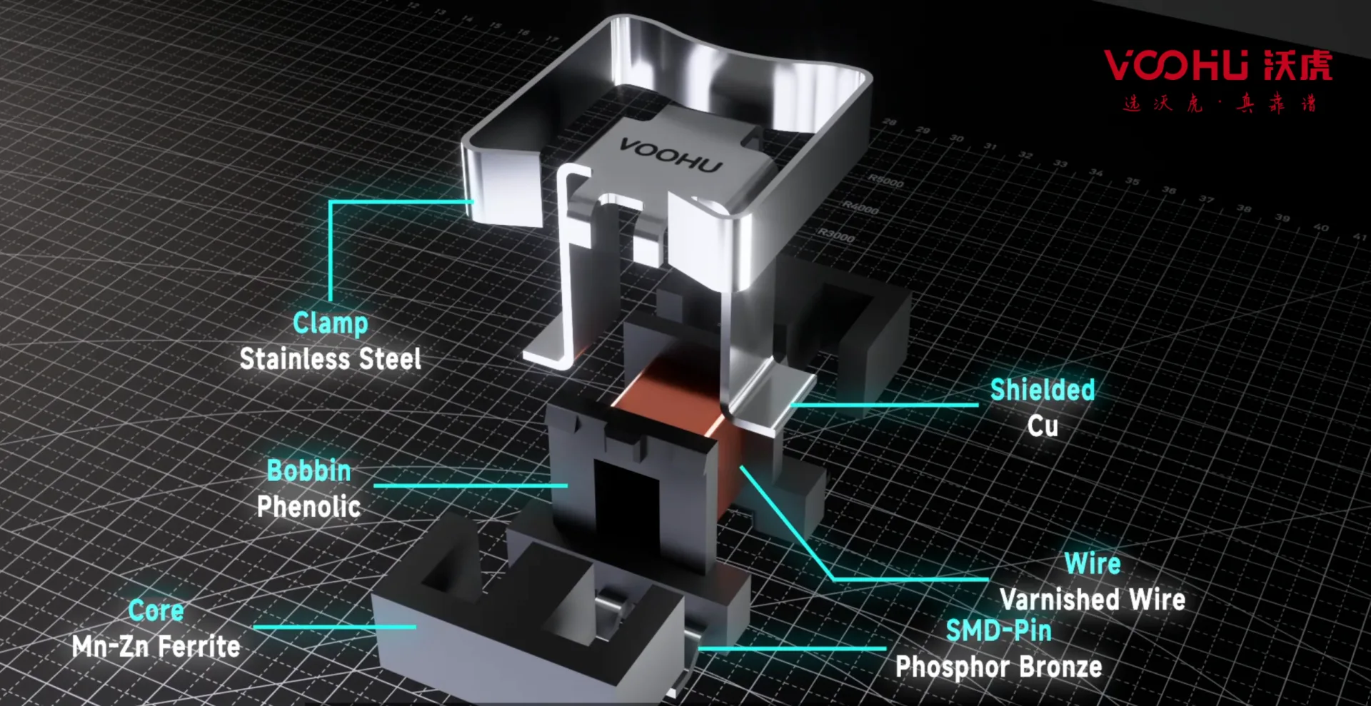
X'fmr+CMC combines the transformer and common mode choke in a chip structure; Cap+CMC combines capacitive coupling and common mode suppression functions according to the official website classification. When selecting, you must first go back to the PHY manufacturer's reference circuit: whether the interface is current type or voltage type, how the center tap is connected, where the terminals and biases are placed, and whether the link requires an independent isolation boundary. These cannot be deduced from the device appearance.
Data rate should be confirmed along with PHY operating mode, cabling, and test methods
Even if they are both 100/1000BASE-T, Cap+CMC cannot be regarded as an unconditional replacement for X'fmr+CMC; safety isolation, voltage withstand and surge paths are still subject to the current specifications and complete machine certification scheme.WHLT-4532B-121MGTThe public fields for 100/1000BASE-T,WHLT-4532B-151MQTFor 2.5G/5G Base-T. The rate field can help narrow the scope, but it is not a substitute for board-level signal integrity checks. Differential pair impedance, trace continuity, number of vias, reference planes, connectors and cables will jointly form a channel; specific trace length, in-pair deviation and return loss limits should be based on the current data of the selected PHY and corresponding part number. When laying out, it is also necessary to make each channel as symmetrical as possible, avoid sudden changes in the reference surface near the magnetic parts, and retain test conditions on the first version board that are convenient for locating problems.
2. PoE bias depends on the published value under DC conditions, not just on the no-load label.
For PoE ports, magnetic components not only carry Ethernet differential signals, but also face DC bias and temperature rise caused by the power supply path.WHLT-4532B-121MGTThe inductance field disclosed on the page is 120 µH @ 10.8 mA DC Bias, and the product title indicates PoE Rating 720 mA;WHLT-4532B-151MQTThe inductance field disclosed on the page is 150 µH @ 10.5 mA DC Bias and marked PoE AT. The inductance values here have clear test conditions and can only be interpreted under the same conditions and topology. The biased values cannot be directly compared horizontally with the no-load inductors on other pages, nor can the available power of the whole machine be derived solely from the word "PoE".
Engineering validation should start with the current path: check the PHY-side and cable-side center taps, power injection locations, current balance across pairs of conductors, and device temperature rise under the most adverse load. If the project requires higher power supply levels, different cable lengths, or higher ambient temperatures, the PSE, PD, connectors, PCB copper thickness, and magnetic components must be reviewed in the same working condition.WHLC-3216A-600M0withWHLC-2012A-801T0The exposed field is a non-PoE direction and should not be put into the power injection path without re-examining the circuitry and current capabilities.
3. Use the shelf material number to create a preliminary list and write down the verification boundaries that cannot be crossed.
The following four material number pages can be accessed normally on the verification date. The speed, combination type, size and inductance or impedance fields in the table are from the official website public page, and their function is to map project requirements to the direction where you can continue to request information. It is not a commitment to substitute materials, nor does it mean that devices in the same package can directly share pads; before placing an order, you should obtain the data sheet, recommended pads and packaging information that are consistent with the material number and version.
| Application and circuit boundaries | Verifiable VOOHU material number | Official website public fields and key verification matters |
|---|---|---|
| Gigabit PoE compact port such as access control or network camera; requires X'fmr+CMC combo | WHLT-4532B-121MGT | 4532B; Focus on checking the PHY reference circuit, bias current path and the most adverse temperature rise. |
| 2.5G/5G PoE access point or edge gateway; higher data rates required | WHLT-4532B-151MQT | 4532B; Focus on verifying the return loss, insertion loss, PoE load and thermal conditions of the complete channel based on current data. |
| Non-PoE 100/1000BASE-T Cap+CMC branch; first confirm that the PHY allows this coupling structure | WHLC-3216A-600M0 | 3216 (1206); Cap+CMC; 100/1000BASE-T; L=60 µH; non-PoE. The product series name alone cannot be used as a substitute for an isolation transformer. The circuit role, pads and certification boundaries need to be confirmed. |
| Smaller size non-PoE Cap+CMC orientation; space priority | WHLC-2012A-801T0 | 2012 (0805); Cap+CMC; 100/1000BASE-T; Impedance 800 Ω; Non-PoE. The impedance test frequency, recommended pads, and actual PHY topology must be confirmed in the current specification before design adoption. |
4. Reflow soldering and placement are not end-of-manufacturing problems, but part of electrical consistency
The really useful part of the preliminary list is to leave out "why you choose it" and "what evidence is still missing" at the same time. For example, Gigabit PoE ports focus on biased magnetic parameters and thermal conditions; 2.5G/5G ports also need to include return loss, insertion loss and PHY equalization capabilities at higher bandwidths for verification; the Cap+CMC direction must first prove that the current PHY reference design allows this coupling structure. Procurement cannot only see a similar part number, but the hardware and manufacturing teams must also see drawings, pads, and test projects that have not yet been closed.
First lock the pad, direction and steel mesh, and then talk about the first article yield
Chip network transformers are small in size and have dense pins. Once the wrong version is used in the pad size, device orientation, Pin 1 marking and steel mesh opening, it may appear as virtual soldering, offset, tombstones or poor consistency between channels. The PCB package library should be checked one by one with the recommended pads of the current material number. General pads cannot be generated based only on the appearance code of 4532B, 3216 or 2012. Before the first piece is mounted, it is recommended that the hardware, PCB library, process and supply chain jointly confirm the material number suffix, packaging direction, nozzle and positioning benchmark, and include the confirmed packaging files into version management.
The reflow curve must be determined by the current data and the actual plate temperature.
The reflow soldering peak temperature, time above liquid phase and temperature rise and fall rate should be based on the current soldering data of the device, solder paste requirements and factory capabilities. Thick copper PoE boards, large ground areas, shields, and adjacent connectors will change the local heat capacity, so the device settings will not equal the true temperature experienced by the device's solder joints. In the first-piece stage, it is advisable to use a temperature measuring board to place points near the device, and use AOI or microscopic appearance to check the wetting, offset, and bridging of the solder terminals. If the link problem only occurs after reflow, the solder joints, inductance changes, device stress, and PCB warpage should also be investigated together to avoid directly attributing it to the PHY software.
5. The layout around magnetic components should take into account differential return paths and noise isolation.
PHY, RJ45, PoE power supply and ESD protection devices are usually present near the Chip LAN. Differential lines should be kept in pairs, continuous and with few detours according to the reference design, and magnetic parts should avoid crossing high dv/dt nodes of switching power supplies or large current pulse loops; the position and grounding path of cable side protection devices should be arranged according to the overall machine protection strategy. There is no fixed distance that applies to all boards. The correct approach is to first identify the noise source, sensitive circuits and chassis ground boundaries, and then use schematic review, near-field inspection and EMC testing to verify whether the layout is established.
6. Break down first article verification into four reproducible board-level steps
The first step is schematic review: Check device roles, center taps, terminations, biasing, PoE injection and ESD paths against the PHY reference design, and confirm the channel number and pin definitions of the selected part number. The second step is assembly review: check the recommended pad, Pin 1, packaging direction, stencil and reflow data, and complete the first piece placement under representative conditions of mass production. The third step is the link matrix: using known normal peers and cables, covering the target rate, negotiation mode, number of ports, temperature, and power supply load, and recording the link start time, disconnection, renegotiation, and project-specified bit error indicators. The fourth step is the worst-case scenario: review the temperature rise, surge, and EMC results under the final chassis, target cables, and actual PoE load.
During mass production handover, hand over the version and test conditions together.
Before the design is frozen, the final part number, data sheet and package diagram versions, PCB library, stencil openings, reflow curves, PHY configuration, PoE load conditions, and link and EMC judgment limits should be synchronized to the procurement, hardware, test, and manufacturing teams. If the PHY, cable, solder paste, or magnetic component suffix is changed in the future, re-verify from the affected boundary instead of relying on the conclusion that "the link was also able to start last time". This will increase the preliminary recording work, but it can significantly reduce the time of misjudgment of welding, power supply and signal problems after mass production.
7. Frequently Asked Questions (FAQ)
Can Chip LAN directly replace traditional network transformers?
It cannot be directly replaced based on package size or product series name. You should first confirm whether the device is X'fmr+CMC or Cap+CMC, and check the center tap, terminal, bias, isolation and surge boundary according to the current PHY reference circuit; the pad, pin definition and certification requirements should also be based on the current information of the corresponding suffix.
When selecting PoE, how to understand the inductor value with DC bias?
The inductance value with DC bias is only valid under the test current and topology conditions noted on the page. It cannot be directly compared with the no-load value of another material number, nor can it be converted into the PoE power of the whole machine alone; the engineering also needs to check the center tap injection path, paired conductor current balance, device temperature rise, and the most unfavorable working conditions formed by PSE, PD, connector and PCB copper thickness.
How should the first round of screening be done for the four on-shelf material numbers?
WHLT-4532B-121MGTIt can be used in 100/1000BASE-T PoE direction first.WHLT-4532B-151MQTFor 2.5G/5G Base-T PoE direction;WHLC-3216A-600M0withWHLC-2012A-801T0It belongs to the non-PoE Cap+CMC direction. This division of labor is only used to narrow the scope of information request. In the end, it is still necessary to combine the PHY topology, current specifications, recommended pads and complete channel testing to determine the materials.
Link problems only occur after reflow soldering, what should be checked first?
First check the solder joint wetting, offset, bridging, stencil opening and device direction, and then check the temperature measurement board records, local heat capacity, PCB warpage and device stress. Then compare the magnetic parameters, chaining and error results before and after reflow; only after the process and device status are eliminated, it is suitable to continue to locate PHY configuration or software problems.
Conclusion
The value of Chip LAN chip network transformers goes beyond reducing the interface area. Only by first distinguishing the roles of X'fmr+CMC and Cap+CMC in the circuit, and then putting the data rate, PHY topology, PoE DC bias, PCB layout and reflow soldering into the same set of first-piece verification, will the size advantage be transformed into a stable mass production solution.WHLT-4532B-121MGT、WHLT-4532B-151MQT、WHLC-3216A-600M0andWHLC-2012A-801T0It can be used as a preliminary reference for the current public shelves; the final decision must still be based on the latest specifications, drawings, delivery dates and physical samples.