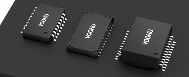

VOOHU gigabit network transformer test and acceptance: VNA fixture, return loss and common mode suppression verification
VOOHU gigabit network transformer test and acceptance: VNA fixture, return loss and common mode suppression verification
The Gigabit Ethernet prototype can negotiate and transmit data normally, which only means that the current board, cable and peer have established a link under this set of conditions. After changing a batch of network transformers, changing a version of the test fixture, or putting the port into an environment with high temperatures, PoE loads, and longer cables, the original occasional packet loss, renegotiation, and radiation problems may still occur. These differences are often collectively referred to as "magnetic component performance fluctuations" at engineering sites. However, without a fixed reference surface, port definition and frequency sweep method, coaxial lines, adapter boards, pads, wiring and contact states are also mixed into the test curve, making the conclusion difficult to reproduce.
Therefore, the acceptance of network transformers should not start with a smooth-looking curve, but should first answer three questions: where is the boundary of the device under test, how does the fixture error move out of the results, and what are the return loss, insertion loss and common mode correlation curves used to judge respectively. The VOOHU Chinese official website can currently check a variety of 100/1000 Base-T single-port and dual-port network transformers. This article uses four public material numbers to establish a test matrix, and connects VNA small signal testing with board-level link, PoE, temperature and insulation verification into a closed loop. The web page fields are only used for preliminary screening; any specific frequency band limits, test levels and judgment lines must still come from the latest specifications, PHY reference designs and project acceptance specifications of the corresponding suffix.
1. First define the DUT boundary and reference surface, and then discuss the quality of the curve.
The reference surface does not fall to the device end, and the curve first reflects the fixture
The VNA establishes a measurement reference plane at the calibration port. If the coaxial line is also connected to an SMA adapter, differential wiring, spring clip or test socket, the instrument will see the overall response of "fixture plus network transformer". The dip in the return loss may come from a connector transition, the slope in the insertion loss may include trace losses, or the anomaly in the common-mode curve may simply be two leg lengths or a solder joint asymmetry. The test report must record the fixture version, connection method, calibration method, port extension or de-embedding file, and DUT welding status; it cannot just save screenshots and part numbers.
It is safer to make reusable test boards for the same package, keep short, symmetrical, and modelable differential channels on both sides of the device, and prepare pass-through or other suitable de-embedding structures. After the calibration is completed, first test the empty fixture or reference piece to confirm the connection repeatability and noise floor, and then load the sample. If the fixture revision, connector batch, welding process or coaxial line changes, the baseline should be re-established and the old judgment tape cannot be used.
Differential reference impedance, port polarity and net naming must be written into the test plan
Gigabit copper links are usually designed around 100 Ω differential systems, but the physical ports of instruments are mostly single-ended 50 Ω. The four-port VNA can first obtain single-ended S parameters and then convert them to differential, common mode and mode conversion parameters according to the correct port pairing. Mismatching port order, positive and negative polarity, or logical port matching can still generate curves, but will distort phase, mode conversion, and channel correspondence. The test plan should draw the PHY side and cable side, the positive and negative ends of each pair, center tap processing and untested port termination methods, and use the reference impedance and frequency band specified in the project data.
2. Return loss, insertion loss and common mode indicators answer different questions
Return loss is used to observe impedance continuity, not a separate device ranking
Return loss is concerned with how much of the incident energy is reflected back by the impedance discontinuity. Device pins, pads, differential traces, fixture transitions, terminations, and winding parasitics can all affect results. The report must also display conventions in a unified manner: some systems use positive values for return loss, and the larger the value, the smaller the reflection; some systems directly display negative values Sdd11 or Sdd22. If the curve names and sign conventions are not stated, the same results may be interpreted in opposite ways. Device acceptance should be compared under the same fixture, the same de-embedding method and the same judgment line, and abnormal locations should be located in combination with the time domain or fixture baseline.
Insertion loss is used to check for valid signal passing but is not a substitute for full link verification
Insertion loss reflects the attenuation of a differential signal from one side to the other. Curve changes may come from winding copper losses, leakage inductance, parasitic capacitance, or ripple caused by fixture traces, connectors, and imperfect matching. Figures obtained with different sweep powers, IF bandwidths, smoothing settings, reference impedances or de-embedding files cannot be directly compared side by side. More importantly, qualified small-signal insertion loss at the device level does not automatically prove that the entire channel composed of PHY transmit amplitude, receiving equalization, RJ45, cables and protection devices has qualified.
Common mode suppression should distinguish between common mode transmission, differential mode conversion to common mode and common mode conversion to differential mode.
Multiple curves are often collectively referred to as CMRR in engineering discussions, but the VNA report should clearly measure whether the mode conversion from differential to common mode, conversion from common mode to differential, or common mode transmission in a certain direction is measured. They are all related to winding balance, pin and fixture symmetry, but are not the same quantity. If you perform a simple differential test with only two physical ports and an external balun, the balun bandwidth, phase amplitude error, and common-mode termination will enter the results, and it will be difficult to fully obtain the mode conversion parameters. When balance characteristics need to be evaluated, calibrated multiport mixed-mode measurements are preferred while retaining the mode conversion margin of the fixture itself.
3. Use public on-shelf material numbers to establish a test matrix instead of writing performance conclusions in advance
The four Chinese official website details pages in the table below will be accessible at the time of verification on August 6, 2026. Only the data rate, installation method, number of ports, pins, spacing, operating temperature, withstand voltage fields and PoE fields that are clearly disclosed on the page are used in the table. The page does not give the complete return loss, insertion loss or common mode curves and their test conditions required for this article, so the table only determines samples, fixtures and subsequent verification branches and does not constitute an interchange, live inventory or volume production suitability commitment.
| Apply borders and fixture branches | Verifiable VOOHU material number | Public fields on the official website and key points for next step verification |
|---|---|---|
| Single port SMD, non-PoE, wide temperature direction; establish Gigabit mixed mode baseline | WHSG24301JM | 100/1000 Base-T; SMD; single port; 24PIN; 1.27 mm; -55℃~+125℃; 1500 V RMS. After obtaining the current specifications, confirm the frequency bands and limits of RL, IL, and mode conversion, and check the cold and hot repeatability. |
| Single port SMD, PoE direction; requires high voltage field preliminary screening | WHSG24701D1 | 100/1000 Base-T; SMD; single port; 24PIN; 1.27 mm; -40℃~+85℃; 5000 V RMS; PoE up to 350 mA. Verify DC bias, temperature rise, center tap, isolation and loaded links. |
| Single port SMD, 4PPoE high current direction; clamp spacing is 1.0 mm | WHSG24R02C0 | 100/1000 Base-T; SMD; single port; 24PIN; 1.0 mm; -40℃~+85℃; 1500 V RMS; 4PPoE up to 1440 mA. Verify DC injection protection, current balance per pair, thermal steady state and load sweep boundaries. |
| Dual-port DIP, PoE+ direction; requires port-by-port and port-to-port verification | WHDG48201P1 | 100/1000 Base-T; DIP; dual port; 48PIN; 2.0 mm; 0℃~+70℃; 1500 V RMS; PoE+ up to 720 mA. Test port by port and check for simultaneous operation, adjacent port coupling, assembly and temperature rise. |
For example,WHSG24301JMThe published temperature range is suitable for establishing a wide temperature sample orientation, but the electrical curves and temperature test conditions must still be confirmed with the current specifications;WHSG24701D1withWHSG24R02C0PoE up to 350 mA and 4PPoE up to 1440 mA are disclosed respectively. These two page fields cannot be directly regarded as the full load temperature rise conclusion of any board;WHDG48201P1It is a dual-port DIP direction. In addition to testing port by port, it is also necessary to evaluate the simultaneous operation of dual ports and the coupling of adjacent ports.
4. Make VNA fixtures, calibration and sample repeatability a traceable process
Review fixtures first, then test gold samples and batches to be inspected
At a minimum, the fixture review includes schematics, stackup, differential line lengths and linewidths, connector models, pads, vias, reference plane continuity, port numbering, and center tap handling. Keep a certified gold fixture and a gold sample for each package. Before starting the test, repeatedly insert, remove and measure the gold sample to see if the curve falls within the established repeatability window; if the baseline drifts, the cable torque, contact, solder joints and temperature should be processed first before judging the sample to be tested.
Calibration and de-embedding must match the fixture structure
Calibration kits are used to remove systematic errors in the instrument and coaxial channels, port extensions compensate for known electrical lengths, and fixture deembedding removes the modelable response of the adapter board. The three have different functions, and one port extension cannot replace all fixture errors. The choice of SOLT, TRL or other methods should be based on the connector, frequency band, available standard parts and laboratory procedures. After de-embedding, check whether there are non-physical gains, sharp breakpoints or abnormal phases to avoid using the wrong fixture model as a device improvement.
Freeze sweep settings and data formats to compare batches
Frequency start and end points, number of points, source power, IF bandwidth, average times, reference impedance, smoothing, time domain gating and mixed-mode port pairing should all be entered into the controlled template. Original Touchstone files, limit lines, instrument status files and result summaries should be stored in conjunction with the material number, suffix, batch, sample number, fixture version and operator. If the production side switches to a faster tester or shortens the frequency sweep points, correlation studies should first be used to prove that it can identify the failures that the design side cares about, rather than simply copying the appearance of a curve.
5. After the VNA is qualified, it is necessary to close the link, PoE, temperature and insulation risks
Network transformers are part of a complete Ethernet channel. After the VNA small signal results are passed, the candidate parts should be soldered to the mass production equivalent board, and a link matrix should be established using the project-approved PHY configuration, RJ45, protection devices, cables, and peers. Cover auto-negotiation, fixed rate, or whatever mode your project requires, record uplink times, retraining, dropouts, and error counts, and retest under target wire lengths, simultaneous port operation, and final chassis conditions. It can only "ping through" under short-term, room temperature, and single-port conditions and cannot replace this closed loop.
PoE devices also need to verify each pair's current flow, center tap connection, current balance, temperature rise and long-term stability under the specified power path and load.WHSG24701D1、WHSG24R02C0withWHDG48201P1The PoE field on the page is used to select the test branch and is not equal to the system power level or the allowable current in any environment. After DC is loaded, the inductance, loss and thermal state of the magnetic components may change; the current should be set according to the current specifications and PoE scheme, and the stable temperature should be recorded under the most unfavorable ambient temperature and port density.
The insulation withstand voltage cannot be derived from the VNA curve either. The Vt value on the page can be used for preliminary screening, but the operating voltage, creepage distance, electrical clearance, test waveform, duration and safety level of the entire machine still need to be independently reviewed. After the withstand voltage or surge test, key electrical parameters and links should be retested to confirm that there is no potential damage. For wide-temperature material numbers, the curve and board-level link tests must be repeated after specifying cold and hot dwells to avoid comparing only room-temperature samples.
6. Four-step inspection process for acceptance of incoming materials from the laboratory
Step 1: Freeze test objects and judgment basis
Lock the complete part number suffix, specification version, PHY reference circuit, project frequency band, differential reference impedance and the official name of each curve. List the sources and judgment conditions of return loss, insertion loss, mode conversion, withstand voltage, PoE, temperature and board-level link respectively; values not given on the public product page should not be filled in by testers themselves.
Step Two: Verify Fixture and Measurement System
Complete the calibration according to the fixed torque and wiring, measure the through structure, empty fixture or verification part specified by the project, and then repeat the measurement of the gold sample. Confirm port mapping, reference planes, de-embedding and mixed-mode conversion are correct, and repeatability windows cover normal fluctuations in connection operations while identifying poor soldering, branch asymmetry or device anomalies.
Step 3: Complete device-level frequency sweep and worst-case board-level combination
Device-level testing saves original S-parameter and limit results; board-level testing covers target PHY, cable, peer, temperature, port density, and applicable PoE load. When encountering curve abnormalities, first use reference parts and time domain positioning to distinguish fixtures, pads, traces, and devices; when encountering link abnormalities, align the VNA results with PHY status, error counts, temperature rise, and power supply noise to avoid attribution based on a single screenshot.
Step 4: Establish the correlation between the design side and the production side
Use qualified samples, boundary samples, and known failure samples to verify the detection capabilities of production testing. The handover document at least includes the material number and suffix, fixture version, calibration cycle, instrument status, source of limit values, golden sample number, retest rules and abnormal upgrade path. If the supply suffix, package, fixture, PHY configuration or PoE conditions change in the future, the relevant items should be re-evaluated instead of inheriting the old conclusion by default.
7. Frequently Asked Questions (FAQ)
If the VNA curve is qualified, can it ensure that the Gigabit link is stable at the target line length?
cannot. The VNA can characterize the linear frequency domain response within the boundaries of the device or fixture, but does not include the full effects of PHY transmit and receive, equalization, RJ45, protection components, cables, software configuration, temperature and power supply noise. It is one of the necessary device-level evidences, and the link matrix and error statistics still need to be completed with a production-equivalent board.
Can return loss and insertion loss measured by different laboratories be directly compared?
Comparability is only possible if frequency bands, reference impedance, port definitions, calibration, fixtures, de-embedding, source power, IF bandwidth, smoothing and display conventions are consistent. The safest way is to exchange original Touchstone files, fixture instructions and gold samples, and do measurement system correlation first.
Is it okay to test only one port of a dual-port network transformer?
Not recommended. Dual-port devices must verify at least two ports separately, and check coupling, simultaneous operation, temperature rise, and assembly consistency between ports based on project risks. If you only test one port, you may miss problems that occur in adjacent channels, common structures, or under dual-port load conditions.
Is it enough for a PoE network transformer to pass the frequency sweep without DC load?
not enough. No-load frequency sweep is suitable for establishing a small signal baseline, but PoE applications must apply the specified current according to the current specification and system plan, and check the current balance, magnetic margin, temperature rise and link stability. The isolation and protection of the VNA port and the DC injection network must also be designed according to laboratory safety procedures, and power supply cannot be directly connected to unprotected instrument ports.
Conclusion
The value of network transformer testing does not lie in generating more curves, but in allowing samples, fixtures, reference surfaces and judgment criteria to be reproduced by the next engineer. First use a controlled fixture to obtain evidence of return loss, insertion loss and mixed mode, and then put the results back into PHY, RJ45, cable, PoE, temperature and insulation boundaries for verification. Only then can "this board be connected to the Internet" be advanced to a deliverable acceptance conclusion.WHSG24301JM、WHSG24701D1、WHSG24R02C0andWHDG48201P1It can be used as a preliminary screening direction for public shelves; before ordering materials, the latest specifications, drawings, delivery dates and physical samples of the corresponding suffix must still be obtained.