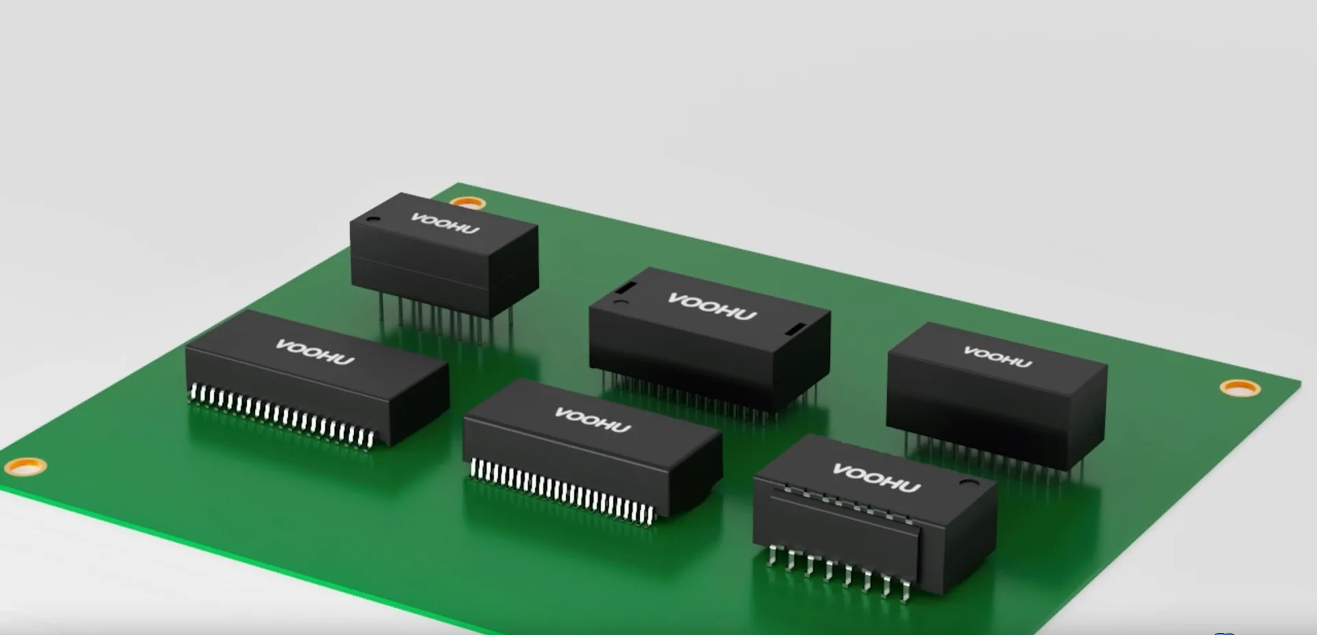

VOOHU Gigabit Network Transformer Packaging Migration: DIP to SMD, Pin Mapping and Mass Production Verification
VOOHU Gigabit Network Transformer Packaging Migration: DIP to SMD, Pin Mapping and Mass Production Verification
Equipment miniaturization, placement automation or supply chain restructuring often put the packaging migration of gigabit network transformers on the agenda. The original board uses DIP devices, and the new board wants to change it to SMD. It seems like just redrawing a pad; but in the actual project, packaging changes will affect both the PHY side and cable side pins, center taps, port sequences, isolation boundaries, differential wiring, assembly processes, and test fixtures. If you only look for alternatives based on "100/1000 Base-T, single port or dual port", the prototype may still be able to start the chain, but problems will be exposed during the PoE loading, temperature rise, EMC or batch assembly stages.
Both the Chinese and English official websites of VOOHU can currently check DIP and SMD 100/1000 Base-T network transformers. This article does not define any two of them as direct replacements. Instead, it uses five public material numbers to explain how to establish a candidate range during package migration, how to check pins on a network-by-network basis, and how to string schematic review, PCB library, trial production, and mass production acceptance into a closed loop. The public page is suitable for the first round of screening; the precise shape, recommended pads, winding diagrams, pin definitions, creepage distances, reflow or wave soldering conditions must be based on the latest specifications and drawings corresponding to the complete suffix.
1. DIP to SMD is not a BOM replacement, but a joint revision of the circuit and process.
The same speed and the same number of ports does not mean that the pins can be translated one by one.
Both sides of the network transformer are connected to the PHY and network port respectively, and the winding may also be equipped with a center tap, common mode processing or PoE power supply path. Even if two devices are labeled 100/1000 Base-T and single port, they may use different pin numbers, spacing, port arrangements, and winding lead-out methods. Before migration, a mapping table must be established based on the network name: list the positive and negative terminals on the PHY side, the positive and negative terminals on the cable side, center taps, shielded or unconnected pins pair by pair, and indicate the original device pins, new device pins and schematic network. The correspondence cannot be guessed based solely on package appearance, total number of pins, or old PCB silk screen printing.
For dual-port devices, you must also confirm the arrangement direction of port A and port B and the channel sequence at both ends. If the port sequence or polarity is reversed, the static continuity check may not be able to detect it immediately, but link training, mode conversion, or EMC results may be affected. During the review, the old schematic, old PCB, candidate device winding diagram and RJ45 definition should be opened at the same time, and reviewed with the netlist or connectivity report instead of relying on manual visual inspection of a pin diagram.
Changes in the installation method will redraw the isolation boundary, and you cannot just redraw the copper skin.
The DIP pins pass through the PCB and the SMD solder terminals are on the same surface. The two structures have different constraints on the pad, solder mask, via holes, copper to board edge distance and test points. After the package is migrated, the area originally naturally stretched by the through-holes may become adjacent pads on the surface; conversely, SMD fan-out may also require via-hole layer changes. The working voltage, electrical clearance, creepage distance and withstand voltage test conditions belong to the safety design of the complete system and cannot be directly derived from the Vt field on the product page. Before the layout is frozen, hardware, PCB and safety personnel should jointly review the latest mechanical drawings, project pollution levels and overall machine standards.
2. Package selection changes differential fan-out, reflow paths, and assembly windows
SMD is good for placement and reflow, but requires more controlled pads and coplanarity
SMD network transformers can usually enter the patch, reflow and AOI processes, reducing through-hole plug-in stations; the cost is that the stencil opening, solder paste volume, placement nozzle, device coplanarity and reflow curve must be re-confirmed. A pad that is too long or the solder paste is uneven may cause the device to shift, stand up, or produce false soldering. A pad that is too narrow may weaken the process margin. The AOI program must also be able to identify pin wetting and bridging, and the blocked areas of the device body may require electrical measurement or sampling X-ray to supplement. Specific pads and temperature profiles must not be copied from another suffix or generic library.
DIP is easy to fix through holes, but it will introduce plug-in, wave soldering and through-hole design constraints
The mechanical fixation and through-hole solder joints of DIP devices are suitable for certain vibration, repair or existing production lines, but they will occupy the through-hole space in the board and increase the control items of plug-in direction, lead shaping, wave soldering shadow, flux cleaning and through-hole filling. After changing to SMD, the original vias cannot simply remain as ordinary vias: they may cut the reference plane, form branches, or crowd out the new differential fan-out. The design team should first determine the assembly route and then decide on packaging, instead of changing the warehouse first and then dealing with process conflicts during trial production.
The differential pair should be short, symmetrical, with few branches, while protecting the continuity of the reference plane.
The area near the network transformer pins is often where the greatest concentration of differential switching layers, center-tap branches, and isolation zones are located. During migration, unnecessary branches and test points should be reduced, the geometric differences between the two branches should be controlled, and whether there is a continuous return path near the layer-changing via hole. When it is necessary to adjust the port direction, give priority to reducing crossovers through device placement and inter-layer planning. Do not stack serpentine lines and dense vias just to "connect". Differential impedance, length tolerance and reference plane requirements are still controlled by the PHY reference design and project rules, and these board-level restrictions are not given on the public product page.
3. Use the actual on-shelf material numbers to determine the migration direction, without preset interchange conclusions.
The five Chinese and English detail pages in the table below have been visited and verified page by page on August 7, 2026. The form takes only the Data Rate, Mounting, Number of Ports, Number of Pins, Spacing, Operating Temperature, Vt, and PoE fields exposed on the page and converts them into design review branches. "On shelf" in this article means that the public details page is currently accessible, and does not represent real-time inventory, delivery or price; any material numbers are not defined as direct replacements because they appear in the same table.
| Migration directions and boundaries | Verifiable VOOHU material number | Official website public fields and next step check |
|---|---|---|
| Single-port SMD, non-PoE, wide temperature direction; suitable for evaluation of placement and high-temperature application branches | WHSG24301GM | 100/1000 Base-T; SMD; single port; 24PIN; 1.27 mm; -40℃~+125℃; 1500 V RMS; non-PoE. Obtain winding diagrams, pin tables, outlines and recommended pads, and check differential pair, center tap, reflow and wide temperature verification conditions. |
| Dual-port SMD, 4PPoE direction; 24PIN structure needs to be checked port-by-port and power supply path | WHSG24Z01C0 | 100/1000 Base-T; SMD; dual port; 24PIN; 1.27 mm; -40℃~+85℃; 1500 V RMS; 4PPoE up to 3000 mA. Check the two-port sequence, center tap, current path for each pair, temperature rise and simultaneous operation. |
| Dual-port SMD, PoE+ direction; 50PIN and 1.02 mm spacing require independent database construction | WHSG50011PG | 100/1000 Base-T; SMD; dual port; 50PIN; 1.02 mm; -40℃~+85℃; 1500 V RMS; PoE+ up to 720 mA. Check the 50PIN lead-out, pad tolerance, AOI visibility, PoE loading and dual-port fixture. |
| Dual-port DIP, non-PoE direction; used as a baseline for through-hole assembly and dual-port migration | WHDG36001TG | 100/1000 Base-T; DIP; dual port; 36PIN; 1.78 mm; -40℃~+85℃; 1500 V RMS; non-PoE. Verify winding and port sequence, hole diameter, plug-in orientation, wave soldering, and dual port operation at the same time. |
| Single port DIP, PoE+ direction; cannot be directly paired with any SMD material number due to 24PIN | WHDG24102PTG | 100/1000 Base-T; DIP; single port; 24PIN; 2.0 mm; -40℃~+85℃; 1500 V RMS; PoE+ up to 720 mA. Check center taps, power paths, vias, and wave soldering conditions before establishing a migration map. |
For example,WHDG24102PTGwithWHSG24301GMAlthough both are single-port 24PIN directions, the public installation method, pin spacing, temperature range and PoE field are different, so the two cannot be regarded as ready-made DIP to SMD pairing.WHDG36001TGThe pin numbers of the two SMD dual-port material numbers are also different, indicating that dual-port migration requires network-by-network mapping.WHSG24Z01C0withWHSG50011PGBoth are SMD dual-ports, but the disclosed 24PIN/50PIN, spacing and PoE fields are still different. Candidate decisions must go back to the system interface, complete specifications and PCB space.
4. Freeze the data first, then complete the schematic and PCB library migration
Step 1: Lock the complete material number suffix and controlled data
The item list should record the manufacturer, complete part number suffix, specification and mechanical drawing versions, date of acquisition, and applicable change notifications. If the supplier page, sample label and PDF suffix are inconsistent, first suspend the database creation and confirm. In addition to the public fields, it is also necessary to obtain winding diagrams, pin definitions, shape tolerances, recommended pads, packaging methods, moisture sensitivity levels and welding conditions; undisclosed items on the page are uniformly marked as "pending technical confirmation" and cannot be completed by similar material numbers.
Step 2: Establish network-by-network pin mapping and reverse review
The mapping table at least contains the old device pins, old network name, functional side, new device pins, new network name, polarity, center tap purpose and reviewer. After completion, first check from the old to the new, and then check from the new to the old to make sure there are no omissions, short circuits or floating. The PoE design must also separately mark each pair of power supply paths, center tap connections, protection and power side connections to avoid mistakenly including non-PoE devices or different current branches as candidates.
Step 3: Create a new library and do three-party cross-checking
The schematic library, PCB package and 3D outline should be created from the same controlled data but examined separately. Library inspection includes pin number, symbol side, pad number, hole diameter or pad size, silk screen foot mark, body forbidden area, assembly origin and height. Then import the netlist into a blank test board, and check the schematic number and PCB pad number pin by pin; then superimpose the mechanical drawing of the candidate device onto the package to confirm the maximum tolerance instead of just looking at the nominal size.
Step 4: Complete layout, DFM and testability countersigns
The layout countersign should cover the differential path from PHY to transformer, transformer to RJ45, center tap and PoE power branch, isolation slot or forbidden area, device height and surrounding maintenance space. DFM countersigning should cover stencil, reflow or wave soldering, AOI visibility, panelization direction, packaging and nozzles; test countersigning should confirm whether the probe point, fixture press fit, boundary scan or functional test can still be executed. Release Gerber and BOM after the three types of countersigning are completed to avoid that the library file is correct but the mass production path is unavailable.
5. Prototype verification must cover signal, power supply, heat and assembly at the same time
Do static connections and device-level electrical checks first
After the first piece is welded, first check the direction, solder joints, open and short circuits and center tap connections, and then perform applicable electrical items according to the latest specifications. If your project requires comparing return loss, insertion loss, or mode conversion, use a controlled fixture and a consistent reference surface, and save the original data, fixture version, and sample number. When the curve is abnormal, first eliminate welding, transition and port mapping problems. Do not directly attribute the difference to the magnetic body.
Shutting down links and PoE risks with production-equivalent boards
Link verification should use the target PHY configuration, RJ45, protection devices, cables, and peers, covering auto-negotiation, project-required rates, target wire lengths, cold starts, warm starts, remating, and error counting. Dual-port devices need to test the two ports separately and add a combination that works simultaneously. PoE candidates must also check the center tap, current balance, chain start-up under load, temperature rise and long-term stability according to the system plan; the "up to" current listed on the website is only used for screening and verification branches, and does not equal the power conclusion that can be directly used by the whole machine.
Let trial production verify placement windows and inspection capabilities at the same time
Small batch trial production should include different board positions and multiple device batches, record process phenomena such as mounting offset, solder joint wetting, bridging, voids or through-hole filling, and correlate AOI, electrical test and functional test results with manual re-judgment. If only the laboratory hand-soldering prototype is verified after changing from DIP to SMD, the risks of offset and virtual soldering during mass production reflow are still not covered. Conversely, if the DIP is retained, plug-in orientation, error proofing, wave soldering shadowing, and rework temperature should also be verified.
The operating temperature and withstand voltage fields also only determine the test branch. In the wide-temperature direction, the chain start-up, error count and key electrical performance must be retested under the cold and hot conditions specified by the project; after the applicable insulation, surge or withstand voltage test is completed, the link and device appearance must be re-checked. System creepage distances, clearances, test voltages, waveforms and durations should be defined by project standards and cannot just reference the 1500 V RMS field on the device page.
6. Four closed-loop inspections before mass production release
Check the information: whether the suffix, drawing, and library version are consistent
BOM, schematic, PCB library, purchase acknowledgment, incoming material label and test specification must point to the same complete suffix. Any temporary materials must be re-mapped and verified, and old conclusions cannot be used because of similar names.
Second check the connection: whether each pair and each center tap is traceable
Save the signed version of net-by-net mapping, netlist difference report and first-piece connection record. For dual-port and PoE designs, there should be separate checks for port sequence, each pair of current paths, and center-tap connections.
Three checks on the process: Whether the placement, welding and inspection windows have been certified by trial production
Confirm that the stencil or wave soldering parameters, device orientation error proofing, AOI or electrical test coverage, repair restrictions, and packaging and loading methods have been verified in small batch trial production, and clarify the acceptable standards and abnormal upgrade paths.
Four performance checks: Whether the device evidence can be associated with the entire machine link
Device-level data, board-level link, PoE load, temperature and insulation results must be bound to the sample, board number and test conditions. If faster and simplified methods are used for production testing, passing, boundary and known failure samples should be correlated to prove that it can identify risks of concern to the design side.
7. Frequently Asked Questions (FAQ)
Both are 100/1000 Base-T, single port 24PIN, can I directly change from DIP to SMD?
Don't draw direct conclusions. Speed, port count, and pin count are just the filtering fields. Also check winding diagram, pin number, center tap, spacing, outline, recommended pad, temperature, withstand voltage, PoE path, and electrical curves. Even if the electrical functionality is similar, changes in installation and assembly methods require re-library building, layout and verification.
Can the 24PIN and 50PIN dual-port SMD network transformers be interchanged by changing the packaging?
You can't just change the package. Pin count differences often mean the pinout, port arrangement, or internal connections need to be reviewed. Winding diagrams and pin tables for both complete suffixes should be obtained, net-by-net mapped and PCB space, differential routing, test fixtures and processes should be re-evaluated.
Can the PoE up to current disclosed on the official website be directly used as the design current of the complete machine?
cannot. This field can be used for initial candidate screening and planning of load testing, but the overall power level, current per pair, center tap, temperature rise, cables, connectors and environmental conditions are determined by the complete system. The current specifications, PoE scheme and thermal test results must be confirmed before ordering materials.
After changing to SMD, is it enough to just verify the new package pads?
not enough. In addition to pads, recheck schematic pins, netlist, isolation boundaries, differential fan-out, reflow profiles, AOI visibility, rework, links, PoE load, temperature, and insulation. Packaging migration is not complete until the design evidence and mass production processes are closed simultaneously.
Conclusion
Package migration requires simultaneous closed-loop material number, pin, PCB library and assembly verification; mass production can only be achieved after trial production, link, PoE, temperature and insulation testing. Formal decision making still requires checking current specifications, drawings, samples and delivery dates.