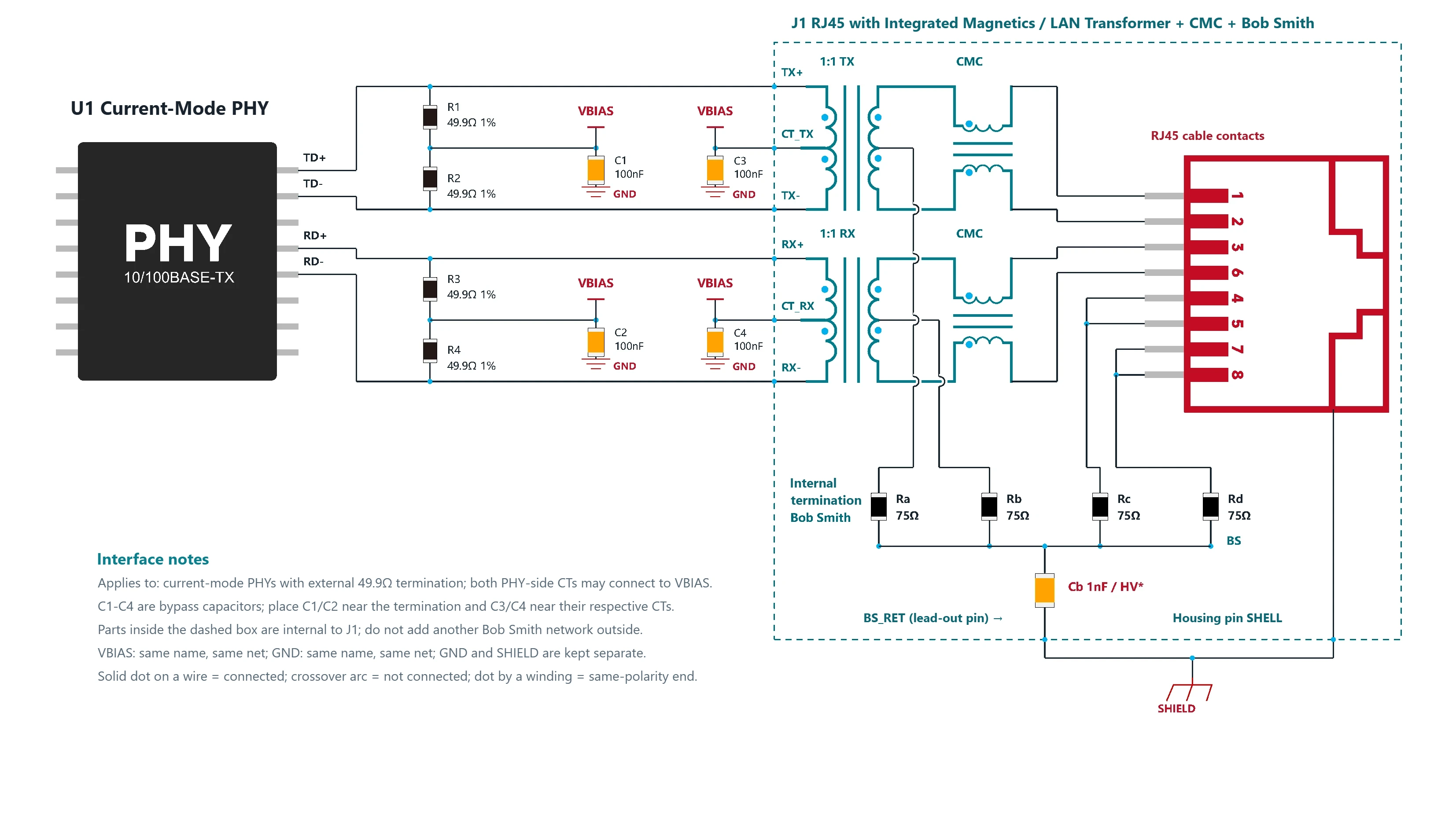
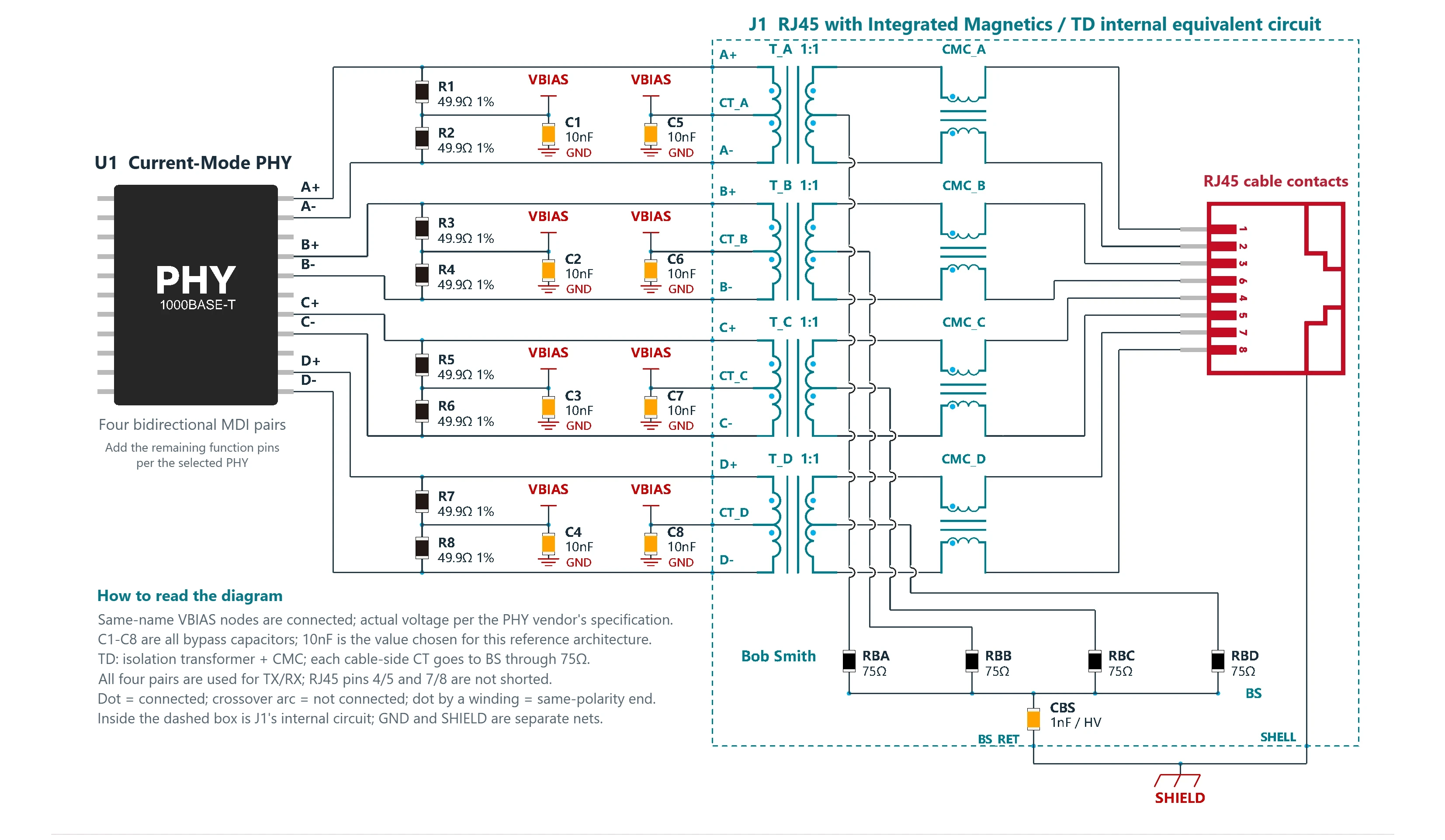
R1–R8 are each 49.9Ω±1%; each of the eight MDI lines connects to VBIAS through its own resistor. The four PHY-side center taps CT_A–CT_D also connect to VBIAS.
Local bypass at every point
C1–C4 sit close to each pair's termination, and C5–C8 sit close to each of the four CTs; each bypasses VBIAS to GND with 10nF. Even on the same supply net, keep a local bypass at each point.
TD structure and four data pairs
Each channel is a 1:1 isolation transformer + CMC. A/B/C/D connect to RJ45 pins 1/2, 3/6, 4/5 and 7/8 respectively; all four pairs carry bidirectional traffic.
Common-mode termination and shield
The four cable-side transformer CTs each go through 75Ω to BS, which connects to SHIELD through CBS (1nF / HV); the metal shell connects directly to SHIELD. The Bob Smith circuit shown is inside J1.
Scope
Non-PoE; for current-mode architectures that use external termination and need a bias supply on the CTs. Confirm VBIAS, the final bypass values and the module specifications for the parts selected. This schematic has no coupling network between GND and SHIELD.
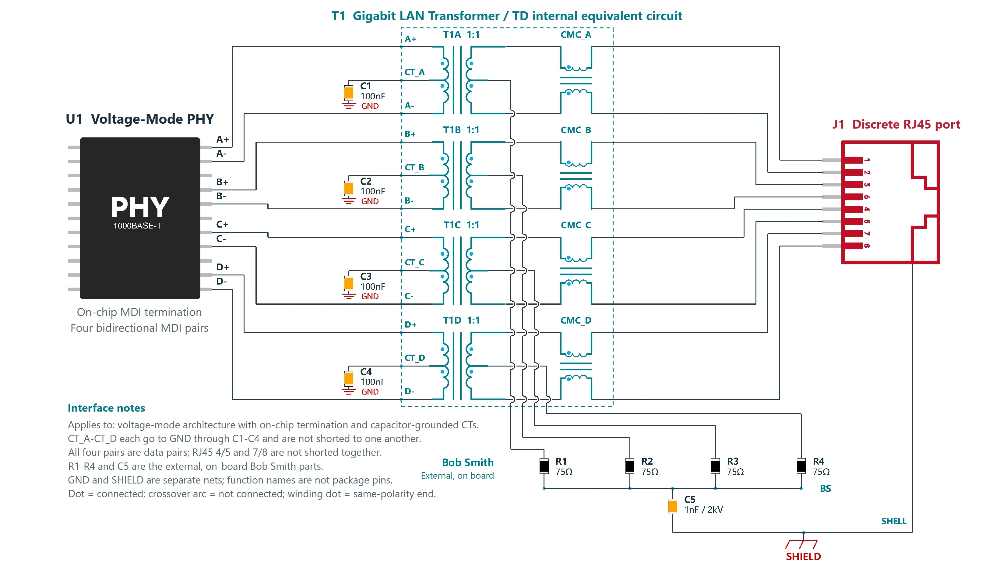
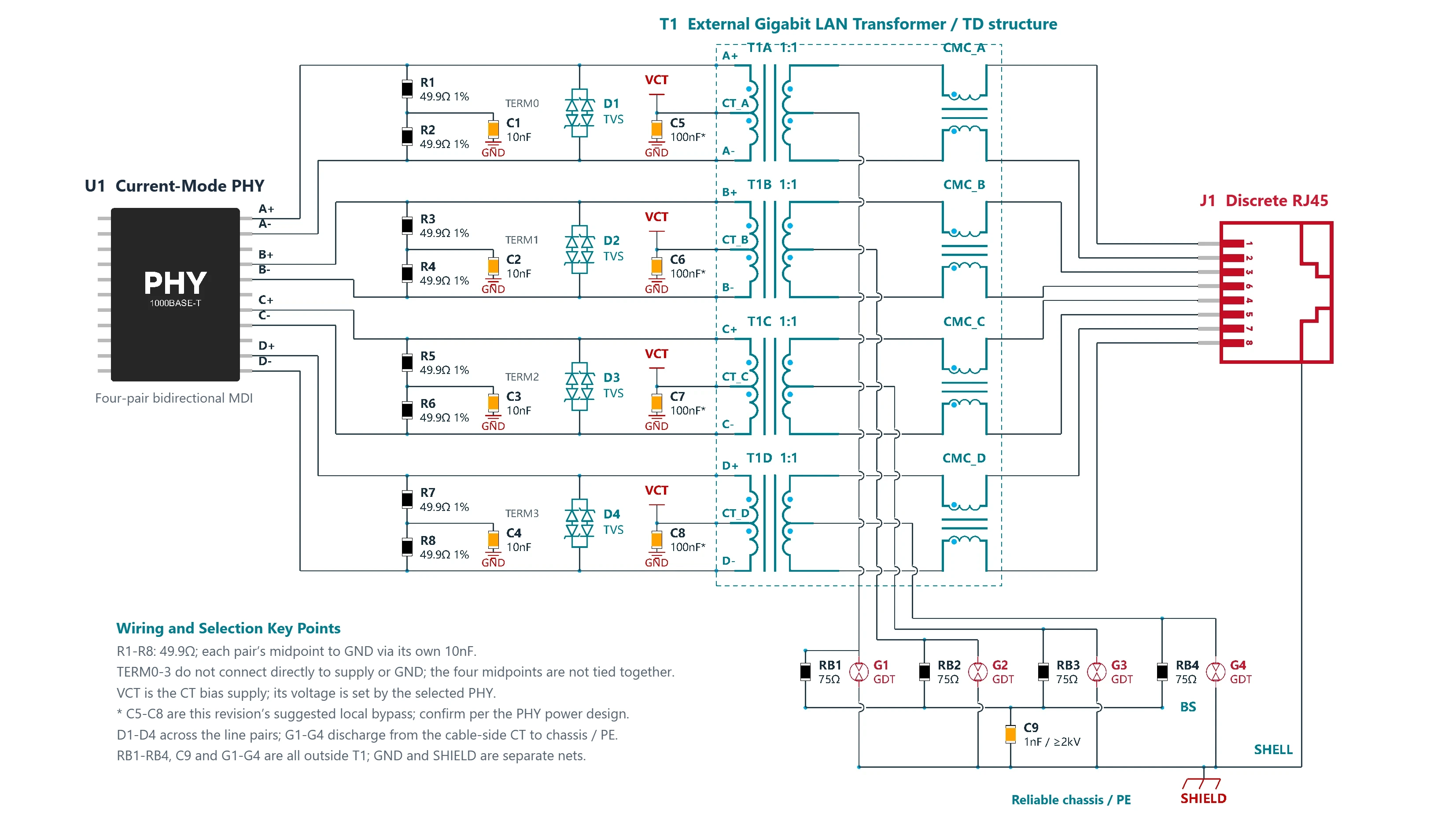
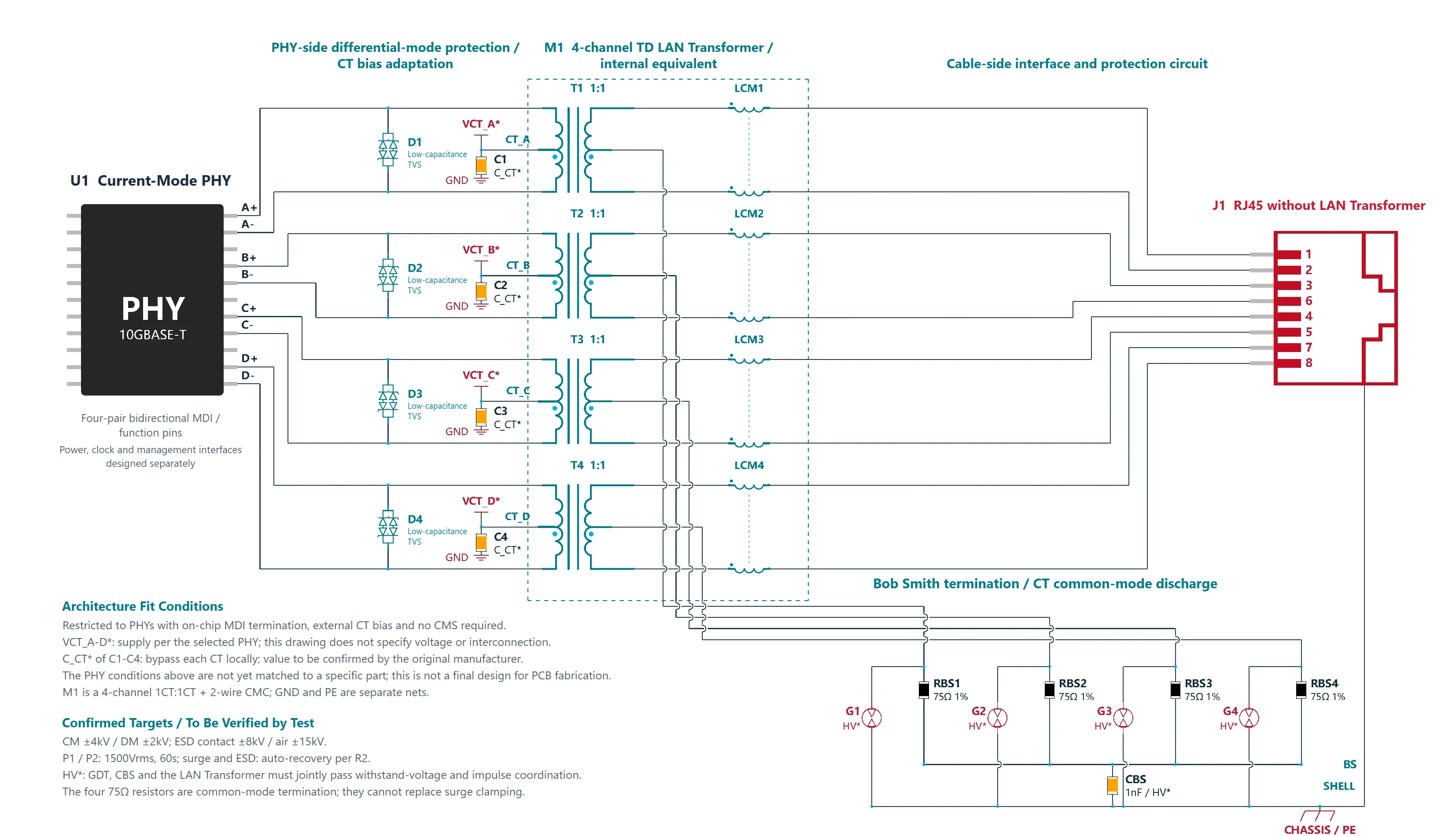
How to read the Gigabit integrated-magnetics RJ45 schematic
All VBIAS nodes of the same name are connected; the actual voltage is as specified by the PHY vendor.
C1–C8 are all bypass capacitors; 10nF is the value used in this reference architecture.
TD: isolation transformer + CMC; each cable-side CT connects to BS through 75Ω.
All four pairs are used for transmit and receive; RJ45 pins 4/5 and 7/8 are not shorted.
Dot = connected; crossover arc = not connected; dot beside a winding = polarity (dotted) terminal.
The dashed box encloses J1's internal circuit; GND and SHIELD are separate nets.
The part numbers above are the VOOHU parts listed under "Product illustrations" in this reference design PDF, for selection reference. Verify the final part numbers item by item against the PHY vendor documentation and the circuit parameters.
Need a quote or samples for these parts? Send your quantity and PHY model to a VOOHU FAE, who will check the part selection against this reference design.
All four MDI pairs carry bidirectional traffic. This schematic is limited to architectures that need external parallel termination and a supply on the PHY-side CTs. Add the remaining power, clock, reset and MAC interface according to the selected PHY.
TI E1 §8; Microchip E2 pp. 2–4
R1–R8 / 49.9Ω±1%
8, outside J1
Pair A: R1/R2; pair B: R3/R4; pair C: R5/R6; pair D: R7/R8. Each line connects to VBIAS through its own resistor, providing the termination and bias for this architecture; the termination midpoint is not connected to GND.
TI E1 p10 Figure 8; Microchip E2 pp. 2–3
C1–C4 / 10nF
4, outside J1
One each for the termination midpoints of A/B/C/D, connected locally between VBIAS and GND to lower the high-frequency impedance of the bias network at the termination. 10nF comes from the reference architecture; it is not a uniform requirement for all PHYs.
TI E1 p10
C5–C8 / 10nF
4, outside J1
Bypass CT_A/CT_B/CT_C/CT_D respectively. The CTs connect directly to VBIAS, and each capacitor is a parallel branch to ground. Place each one locally; do not merge them into one just because they share the same supply name.
TI E1 p10 Figure 8
VBIAS / bias net
Same-name nodes connected
Provides the required bias for the eight termination resistors and the four PHY-side CTs. Confirm the voltage and its allowed maximum against the PHY; this schematic does not fix it at 3.3V, and does not treat this net as circuit ground.
TI E1 p10; Microchip E2 pp. 2, 4
T_A–T_D / 1:1
4 channels, inside J1
Carry the differential signals and isolate the PHY from the cable. The PHY-side CTs connect to VBIAS; each cable-side CT goes to its own 75Ω. The turns ratio is 1:1; inductance, loss, crosstalk and isolation conditions must match the PHY.
Microchip E2 pp. 3–4; Microchip E4 p5 Figure 3
CMC_A–CMC_D
4 channels, inside J1
A two-winding common-mode choke in series on the two cable-side data lines, forming a TD channel with the isolation transformer; it suppresses common-mode noise. Its differential-mode insertion loss and frequency response must also meet the signal requirements.
Microchip E4 pp. 4–5, Figure 3
TD / four magnetics channels
4×T + 4×CMC
In this schematic, TD means an isolation transformer plus a common-mode choke, with no autotransformer winding. Bob Smith termination is taken from the transformer's cable-side CT, before the CMC; the PHY-side CT stays isolated from it.
Microchip E4 p5 Figure 3; Microchip E2 p4
RBA–RBD / 75Ω
4, inside J1
Connect the cable-side CTs of T_A/T_B/T_C/T_D to the common BS node respectively. Each of the four channels passes through its own 75Ω before they join, forming the common-mode termination; the four CTs must not be shorted together first. Do not add them again externally.
Microchip E2 p4; Microchip E4 p5 Figure 3
CBS / 1nF, HV
1, inside J1
BS is AC-coupled to SHIELD through this capacitor, which also blocks DC in this branch. 1nF is from E1/E2; the E1 example uses 3kV and E2 uses 2kV. Confirm the final voltage rating and test conditions for the module; this capacitor cannot serve as a surge clamp.
TI E1 p11; Microchip E2 p4
J1 / RJ45 and shield shell
1 integrated module
A→1/2, B→3/6, C→4/5, D→7/8, all data pairs. SHELL connects directly to SHIELD; the dashed outline shows which parts belong to the module. The module shown contains four TD channels, the 75Ω resistors and CBS; confirm each item when selecting the part.
Microchip E2 pp. 4–5; Microchip E4 §3.8
GND / SHIELD
Two separate nets
GND is the PHY circuit ground; the shield side of CBS and the metal shell both connect to SHIELD. This schematic does not define how GND, the chassis and PE relate at the system level, and draws no additional RC coupling branch.
TI E1 p11; Microchip E2 p5
Vendor documentation and scope of use
E1 · Texas Instruments AN-1263 / SNLA056D, Rev. D, 2013, pp. 10–11. Used only for external termination, CT bias and local bypassing; the TDA figure on p14 is not used as the basis for the TD structure in this version.
E2 · Microchip / SMSC LAN8810 QFN Schematic Checklist, Rev. B, 2014, pp. 2–5. Used to cross-check termination, CT supply, pair mapping, Bob Smith and shielding.
E3 · Motorcomm "YT8511 Application Note" V1.2, p3, a public repost attributed to the vendor. That document describes a voltage-mode PHY with on-chip termination; it is used only to rule out that architecture, not as the basis for this schematic's current-mode connection.
E4 · Microchip / Microsemi ENT-AN0098 / VPPD-01740, Rev.2.2, 2018-06, body text pp. 4–5 (PDF pp. 6–7), Figure 3. Used only for the TD structure with a cable-side two-winding CMC and for where the CT termination connects; the PHY-side CT supply still follows E1/E2.
Limits of use
This schematic is a non-PoE MDI interface reference circuit. After the actual PHY and RJ45 with integrated magnetics are selected, re-check the parameters, package pin numbers and system grounding, and carry out link, MDI, EMC and insulation validation. The review in this document does not replace hardware testing.
Gigabit integrated-magnetics RJ45 circuit FAQ
Should the center taps of a current-mode Gigabit PHY connect to 3.3V?
They need a bias supply, but not necessarily 3.3V. In this schematic, the four PHY-side center taps (CT_A–CT_D) and the eight 49.9Ω termination resistors all connect to VBIAS, and C5–C8 each bypass locally to GND with 10nF. Confirm the VBIAS voltage and its allowed maximum against the selected PHY's vendor documentation. This schematic does not fix VBIAS at 3.3V, and does not treat VBIAS as circuit ground.
Can the midpoint of the 49.9Ω termination resistors be tied directly to ground?
No. In this schematic, each MDI line connects to VBIAS through its own 49.9Ω±1% resistor (pair A: R1/R2, pair B: R3/R4, pair C: R5/R6, pair D: R7/R8). The termination midpoint is not connected to GND; C1–C4 (10nF) bypass VBIAS to GND locally. This connection applies only to current-mode architectures that need external parallel termination and a supply on the CTs.
C1–C8 are all 10nF and all on VBIAS. Can they be merged into one or two capacitors?
Merging them is not recommended. C1–C4 sit close to each pair's termination midpoint, and C5–C8 sit close to each of the four CTs. Even on the same supply net, keep a local bypass at each point; do not merge them into one just because they share the same supply name. 10nF is the value used in this reference architecture, not a uniform requirement for all PHYs; confirm the final bypass values for the parts selected.
With an RJ45 with integrated magnetics, do I still need to add the Bob Smith 75Ω and 1nF on the board?
This schematic does not add them again externally. The J1 integrated module shown contains four TD channels, RBA–RBD (75Ω) and CBS (1nF/HV): the four cable-side CTs each go through 75Ω to BS, which connects to SHIELD through CBS, forming the Bob Smith common-mode termination. However, whether a module actually contains these components, and their voltage ratings, must be confirmed item by item against the selected module's specifications.
What does the TD magnetics structure mean here? Should RJ45 pins 4/5 and 7/8 be shorted?
TD means a 1:1 isolation transformer plus a cable-side two-winding common-mode choke (CMC) in each channel, with no autotransformer winding; Bob Smith termination is taken from the transformer's cable-side CT, before the CMC. 1000BASE-T uses all four pairs for bidirectional traffic, with A/B/C/D connected to RJ45 pins 1/2, 3/6, 4/5 and 7/8 respectively, so 4/5 and 7/8 are not shorted.
Hello! Thank you for using the VOOHU official platform
To provide you with more accurate technical support, please fill in the following information
*We promise to strictly keep your information confidential, only for material delivery and follow-up technical support
Submission Successful
Thank you for your trust and support. Our engineering team will contact you within 1 business day to provide product selection recommendations and technical support
Talk to VOOHUWeekdays 8:30–18:00 (UTC+8) · first reply within 1 business day
Keep the site secure and working, and remember your language and cookie choice.
VOOHU
02
Analytics
Show us which pages are visited and how the site performs, so we can improve it.
Google Analytics · Ahrefs · VOOHU
03
Ad measurement
Measure which of our campaigns bring visitors to VOOHU.
Google Ads
04
Ad personalization
Show you more relevant VOOHU ads on other websites.
Google Ads · Meta · LinkedIn
In the EEA, the UK and Switzerland, analytics and advertising stay off until you allow them. Elsewhere, Google Analytics and Google Ads measurement are on by default, and ad personalization stays off until you allow it.
Changes save automatically
Privacy
Your privacy, your choice
We use cookies to run this site, understand how it’s used and measure our campaigns. Choose what’s on, and change it anytime in Cookie settings. Cookie Policy
✓Preferences saved. Change them anytime under Cookie settings in the footer.
WhatsApp Chat
Typically replies in minutes
Support
Hi! Thank you for connecting with VOOHU! How can we help you today?
Online now
We’ll open WhatsApp (mobile app or WhatsApp Web) with your message pre-filled.


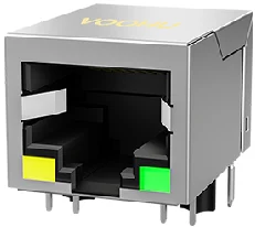 RJ45 with integrated magnetics (for J1, the integrated network interface)SYT-320DNLView SYT-320DNL →
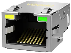 RJ45 with integrated magnetics (for J1, the integrated network interface)SYT211Q106-DB1A7CBS057View SYT211Q106-DB1A7CBS057 →
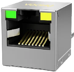 RJ45 with integrated magnetics (for J1, the integrated network interface)SYT511Q070-AB1A8DView SYT511Q070-AB1A8D →
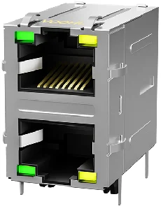 Two-tier stacked RJ45 with integrated magnetics (for J1, the integrated network interface)SYT21Q042-DB2A4D068View SYT21Q042-DB2A4D068 →