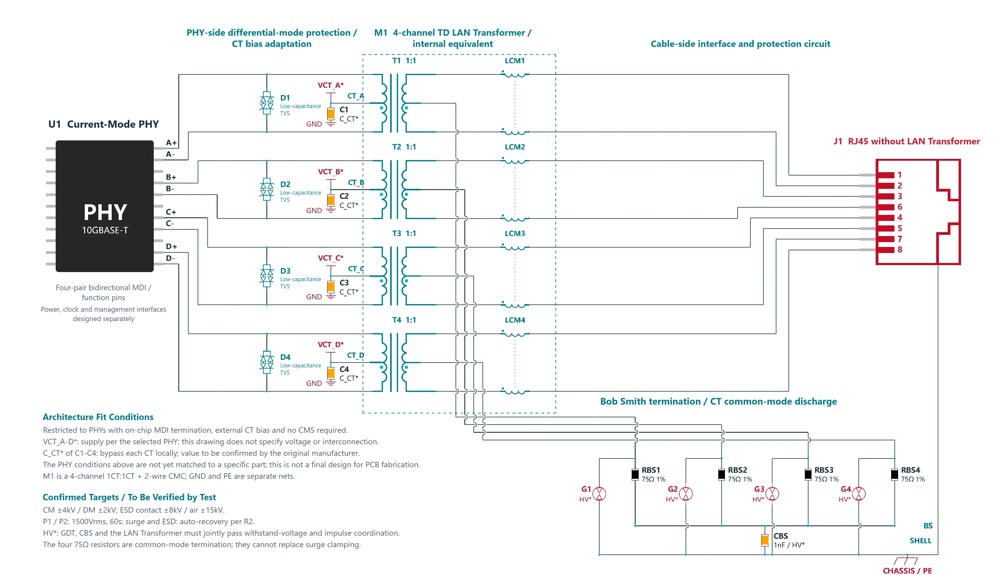
10GBASE-T Lightning Surge Protection for Current-Mode PHY: TVS + GDT Reference Design · Standard reference design schematic (D1.2)
Key points of lightning surge protection for a 10G current-mode PHY
Structure and conditions of use
Non-PoE; discrete shielded RJ45, external four-channel LAN transformer, and a reliable chassis ground/PE. The main schematic is limited to PHY architectures with on-chip MDI termination, CTs that need an external bias, and no CMS required. Matching to a specific part number and its supporting parameters is not yet complete; this is currently a revised-architecture draft.
Data interface and CT bias
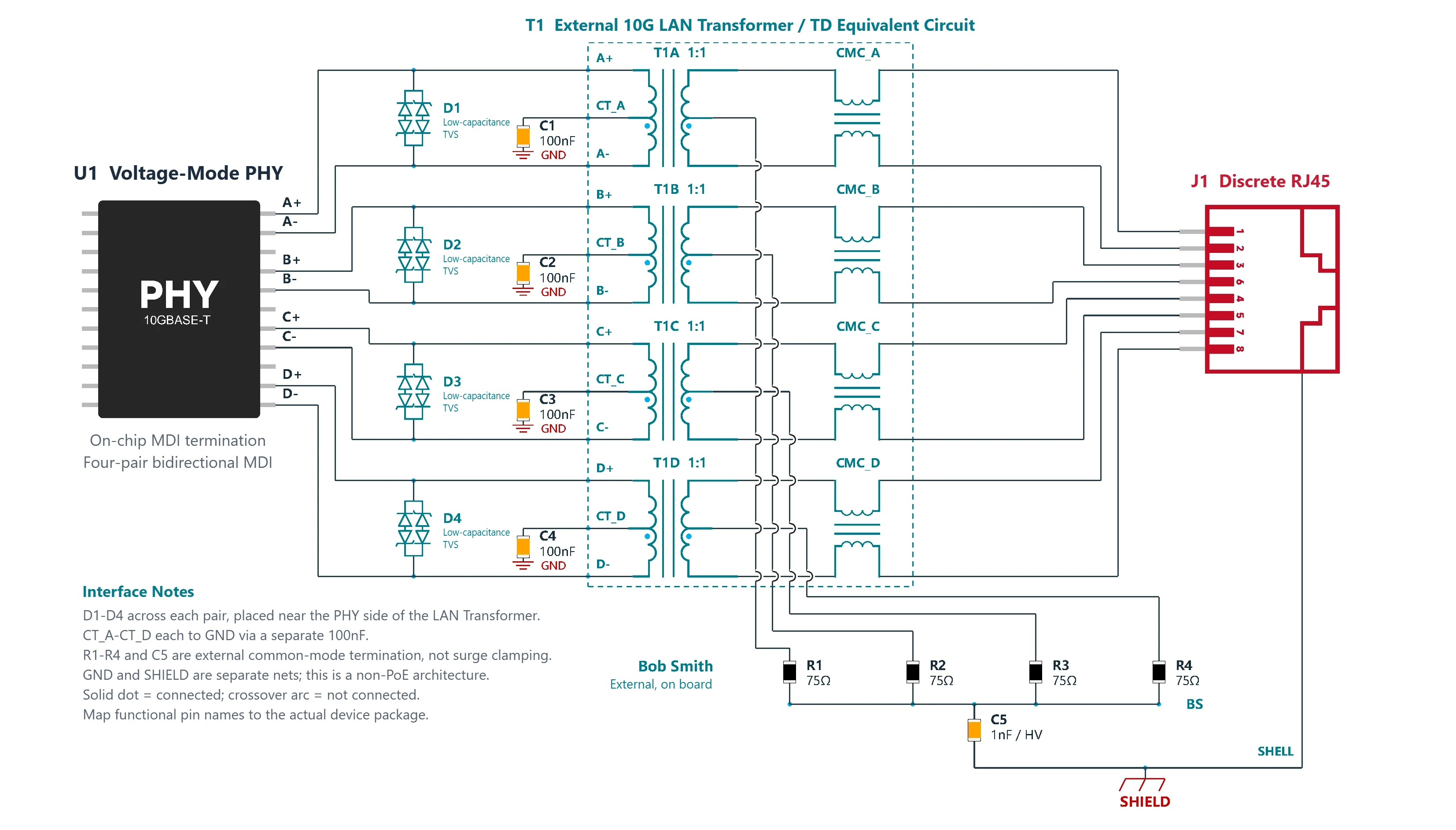
A–D are four bidirectional MDI pairs, connected in order to RJ45 pins 1/2, 3/6, 4/5 and 7/8. VCT_A–D each denote a CT bias that is still to be confirmed; C1–C4 each bypass to GND close by. The voltage, the capacitance, and whether the CTs can share one supply are all set by the selected PHY's vendor schematic.
Isolation and common-mode termination
M1 is a four-channel 1CT:1CT isolation LAN transformer with two-wire CMCs on the cable side. Each of the four cable-side CTs goes through 75Ω to BS, which connects to chassis ground through CBS (1nF/HV*); the four channels are laid out symmetrically. All eight contacts carry data.
Protection and return path
D1–D4 are each connected across one PHY-side differential pair. G1–G4 connect the cable-side CTs to PE and must meet both the high withstand-voltage requirement and dynamic discharge coordination; do not assume they are low-voltage discharge tubes. The metal shell connects directly to the same PE; circuit GND is a separate net. The Bob Smith network does not replace surge protection.
Design targets and implementation limits
W1: common-mode ±4kV, differential-mode ±2kV; E4: contact ±8kV, air ±15kV. P1 and P2 are both 1500Vrms/60s; surge and ESD both follow R2 automatic recovery. These are test targets; PHY matching, protection part selection and system-level results still need validation.
How to read the 10G current-mode PHY surge protection schematic
Limited to PHYs with on-chip MDI termination, external CT bias, and no CMS required.
VCT_A–D*: supplied as the selected PHY requires; this schematic does not specify the voltage or interconnection.
C_CT* for C1–C4: a local bypass for each CT; confirm the value from the vendor documentation.
The PHY conditions above have not yet been matched to a specific part number; this schematic is not a final design for PCB fabrication.
M1 is four 1CT:1CT channels + two-wire CMCs; GND and PE are separate nets.
HV*: the GDTs, CBS and LAN transformer must together pass withstand-voltage and impulse coordination.
The four 75Ω resistors are common-mode termination; they cannot replace surge clamping.
Functional pin names are not solder pin numbers; the dashed box shows M1's internal functions. Pins with the same name are connected; solid dots are connections, crossover arcs are not; the dashed line on a CMC indicates magnetic coupling.
Note: four-channel revised-architecture draft. PHY bias/termination matching is not yet closed, and protection and 10G performance must be validated; not ready to send to PCB fabrication as is.
GDT gas discharge tube (for G1–G4, cable CT to PE; withstand voltage must be confirmed against P2)WHGD200V1P0BView WHGD200V1P0B →
The part numbers above are the VOOHU parts listed under "Product images" in this reference design PDF, for selection reference. Verify the final part numbers item by item against the PHY vendor documentation and the circuit parameters.
Need a quote or samples for these parts? Send your quantity and PHY model to a VOOHU FAE to check the part selection against this reference design.
This schematic assumes on-chip termination, externally supplied CTs and no CMS required. No specific PHY vendor schematic that meets all these conditions has been found yet. The VCT voltage/interconnection and any need for external termination must not be inferred from the PHY type name. Not to be used as a schematic for PCB fabrication.
PHY source still to be added; [7][8] for comparison only
M1 / T1–T4; LCM1–LCM4
4 × 1CT:1CT; 4 × two-wire CMC
Only the four data magnetics channels are kept; the CMCs are on the cable side, and each CT is brought out directly and independently. The internal function designators are not eight external BOM parts. Re-match the magnetics to the actual PHY and the 10G link.
[1]; Matching to be validated
C1–C4 / C_CT*
4 × CT bypass; value to be confirmed
Each connects its pair's VCT to circuit GND and sits close by. Do not assume a shared supply, and do not assume 2.5V or 4.7µF. After selecting the PHY, confirm the capacitance, voltage rating, effective capacitance and supply decoupling.
PHY vendor schematic to be determined
RBS1–RBS4
4 × 75Ω 1%
The four cable-side CTs go through 75Ω each to BS, and CBS blocks DC on the return to the chassis; this provides common-mode termination. The 1% tolerance is an engineering choice.
[2]
CBS
1nF / HV*
Pulse energy, the AC/impulse capability of CBS, and parasitics are still to be validated; 1nF does not indicate a protection level.
Tolerance/HV*: engineering acceptance criteria
D1–D4
4 × low-capacitance bidirectional; across pairs on the PHY side
Suppress differential-mode stress reaching the PHY side. The working voltage must cover the signal, the residual voltage must stay below the PHY's transient limit, and parasitics/energy must be checked. The vendor's 500V example cannot be extrapolated to show that this version passes 2kV differential-mode.
[2]; Part still to be selected
G1–G4 / HV*
4 × high-voltage GDT; cable CT to PE
Must withstand P2 in the assembled state without firing, and the maximum dynamic sparkover voltage must be checked. A high-voltage GDT may not fire within 4kV; the LAN transformer, CBS and spacing cannot rely on it always conducting, and a 5kV engineering margin must be verified.
[3][4]; Engineering extension
J1 / GND / PE
Shielded RJ45 without LAN transformer; non-PoE
1/2, 3/6, 4/5 and 7/8 remain four complete differential pairs; the shell connects directly to a reliable chassis PE. Circuit GND is a separate net; the cable-side CT return path and protection parts do not bridge to PHY-side GND.
[1][2]; System grounding design
Surge W1 / R2
Test conditions and acceptance targets for this version
CM ±4kV: common mode on all 8 lines, 40Ω coupling + 2Ω source. DM ±2kV: the two lines of each pair in turn, through a project-added 42Ω floating loop.
Coupling and waveform
Test conditions and acceptance targets for this version
CM is calibrated per IEC Table 10; at 4kV, the total Isc is nominally 96A. 10G transparency is verified separately. The generator's 8/20µs is not the same as the CDN output waveform.
ESD E4 / R2
Test conditions and acceptance targets for this version
Contact ±8kV, air ±15kV; includes the applicable accessible points and indirect discharge. See the full test specification for test points and number of discharges.
P1 / P2 / R2
Test conditions and acceptance targets for this version
P1 and P2 are both 1500Vrms, 50/60Hz, 60s, with all protection parts fitted. Engineering limit: 10G must recover automatically within 60s; manual reset is not allowed.
Vendor documentation and scope of use
[1] · Bel S558-10GB-05, electrical diagram Rev.E / 2020-06-29, downloaded PDF p. 1
[3] · Littelfuse General Port Protection Spotlight, 2024, p. 8 / p. 10
[4] · Bourns GDT28H, p. 1: AC withstand voltage, impulse sparkover voltage and surge ratings
[5] · IEC 61000-4-5:2014+A1:2017; checked against the 2014 main text, §6.3.3.3 and Tables 9/10
[6] · IEC 61000-4-2:2025; system-level contact/air and indirect discharge methods
[7] · Intel X540 Datasheet v3.1, §13.2.2–13.2.4, §13.2.8 (comparison used to rule out)
[8] · Intel X550 Datasheet Rev2.7, §13.2.7 / p. 1148 (comparison used to rule out)
Limits of use
The four-channel magnetics structure is checked against Bel's original drawing; the common-mode termination and protection methods follow Semtech and other vendor documentation. The basis for a specific current-mode PHY, its bias and its termination is not yet closed. This is currently an architecture diagram limited to stated matching conditions, not a copy of a validated reference board. Validation scope and status: four-channel revised-architecture draft; PHY basis not yet closed. Document, connection and asset checks are complete; no native EDA ERC or physical testing has been done. For the VCT*, C_CT* and termination matching in the main schematic, a specific PHY vendor schematic must be obtained first, and only then can a version ready for PCB fabrication be produced. The confirmed protection targets remain unchanged; Cat6A U/UTP is the test baseline, and the 5kV margin and 60s recovery limit are engineering conventions. The product display keeps only the original images and part numbers and is not a compatibility conclusion.
What is the CT bias voltage for a 10G current-mode PHY? Can all four CTs share one supply?
This schematic does not specify it. VCT_A–D* are supplied as the selected PHY requires. The voltage, the interconnection, and whether the CTs can share one supply are all set by the selected PHY's vendor schematic; they must not be inferred from the type name "current-mode". C1–C4 each bypass their pair's VCT to GND close by; a shared supply is not assumed, and neither is 2.5V or 4.7µF.
Can this 10G current-mode protection schematic go straight to PCB fabrication?
No. It is the D1.2 four-channel revised-architecture draft, limited to PHYs with on-chip MDI termination, CTs that need an external bias, and no CMS required, but no specific PHY vendor schematic that meets all these conditions has been found yet. So far only document, connection and asset checks have been done; no native EDA ERC or physical testing has been performed. A specific PHY vendor schematic must be obtained first, and only then can a version ready for PCB fabrication be produced.
How should the voltage rating be chosen for the GDTs from the cable-side center taps to PE?
Choose a high-voltage GDT (gas discharge tube); do not assume a low-voltage discharge tube. G1–G4 connect the cable-side CTs to PE. In the assembled state they must withstand P2 (1500Vrms, 50/60Hz, 60s) without firing, and their maximum dynamic sparkover voltage must be checked. A high-voltage GDT may not fire within 4kV, so the LAN transformer, CBS and spacing cannot rely on it always conducting; a 5kV engineering margin must be verified.
What does each part do: the PHY-side TVS diodes, the cable-side GDTs and the Bob Smith 75Ω resistors?
D1–D4, low-capacitance bidirectional TVS (transient voltage suppressor) diodes, are connected across the PHY-side differential pairs and suppress differential-mode stress reaching the PHY; their residual voltage must stay below the PHY's transient limit. G1–G4, high-voltage GDTs, sit between the cable-side CTs and PE. RBS1–RBS4, four 75Ω resistors, return to the chassis through CBS and provide common-mode termination only; they cannot replace surge clamping.
What are this version's surge and ESD targets, and does it already pass them?
It has not passed; these are test targets only. Surge W1: common-mode ±4kV, differential-mode ±2kV. ESD E4: contact ±8kV, air ±15kV. P1/P2: both 1500Vrms/60s. For surge and ESD, R2 requires 10G to recover automatically within 60s, with no manual reset. PHY matching, protection part selection and system-level results still need validation.
Hello! Thank you for using the VOOHU official platform
To provide you with more accurate technical support, please fill in the following information
*We promise to strictly keep your information confidential, only for material delivery and follow-up technical support
Submission Successful
Thank you for your trust and support. Our engineering team will contact you within 1 business day to provide product selection recommendations and technical support
Talk to VOOHUWeekdays 8:30–18:00 (UTC+8) · first reply within 1 business day
Keep the site secure and working, and remember your language and cookie choice.
VOOHU
02
Analytics
Show us which pages are visited and how the site performs, so we can improve it.
Google Analytics · Ahrefs · VOOHU
03
Ad measurement
Measure which of our campaigns bring visitors to VOOHU.
Google Ads
04
Ad personalization
Show you more relevant VOOHU ads on other websites.
Google Ads · Meta · LinkedIn
In the EEA, the UK and Switzerland, analytics and advertising stay off until you allow them. Elsewhere, Google Analytics and Google Ads measurement are on by default, and ad personalization stays off until you allow it.
Changes save automatically
Privacy
Your privacy, your choice
We use cookies to run this site, understand how it’s used and measure our campaigns. Choose what’s on, and change it anytime in Cookie settings. Cookie Policy
✓Preferences saved. Change them anytime under Cookie settings in the footer.
WhatsApp Chat
Typically replies in minutes
Support
Hi! Thank you for connecting with VOOHU! How can we help you today?
Online now
We’ll open WhatsApp (mobile app or WhatsApp Web) with your message pre-filled.


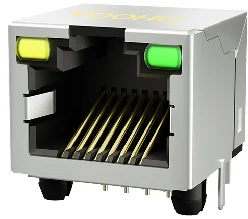 Discrete shielded RJ45 (for J1, no LAN transformer)SYT561188-AB1A3DY1027View SYT561188-AB1A3DY1027 →
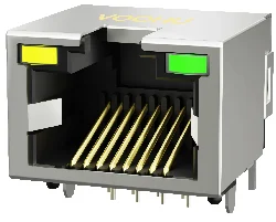 Discrete shielded RJ45 (for J1, no LAN transformer)SYT60S1188-AB1A6DY1008View SYT60S1188-AB1A6DY1008 →
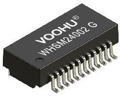 External 10G LAN transformer (for M1, four-channel TD-structure transformer)WHSM24002GView WHSM24002G →
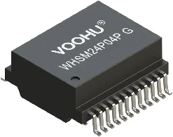 External 10G LAN transformer (for M1, four-channel TD-structure transformer)WHSM24P04PGMore LAN transformers →
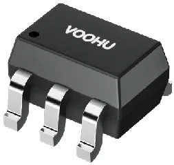
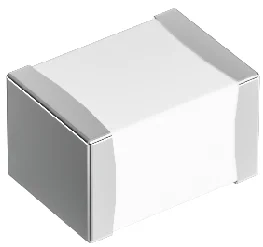 GDT gas discharge tube (for G1–G4, cable CT to PE; withstand voltage must be confirmed against P2)WHGD200V1P0BView WHGD200V1P0B →