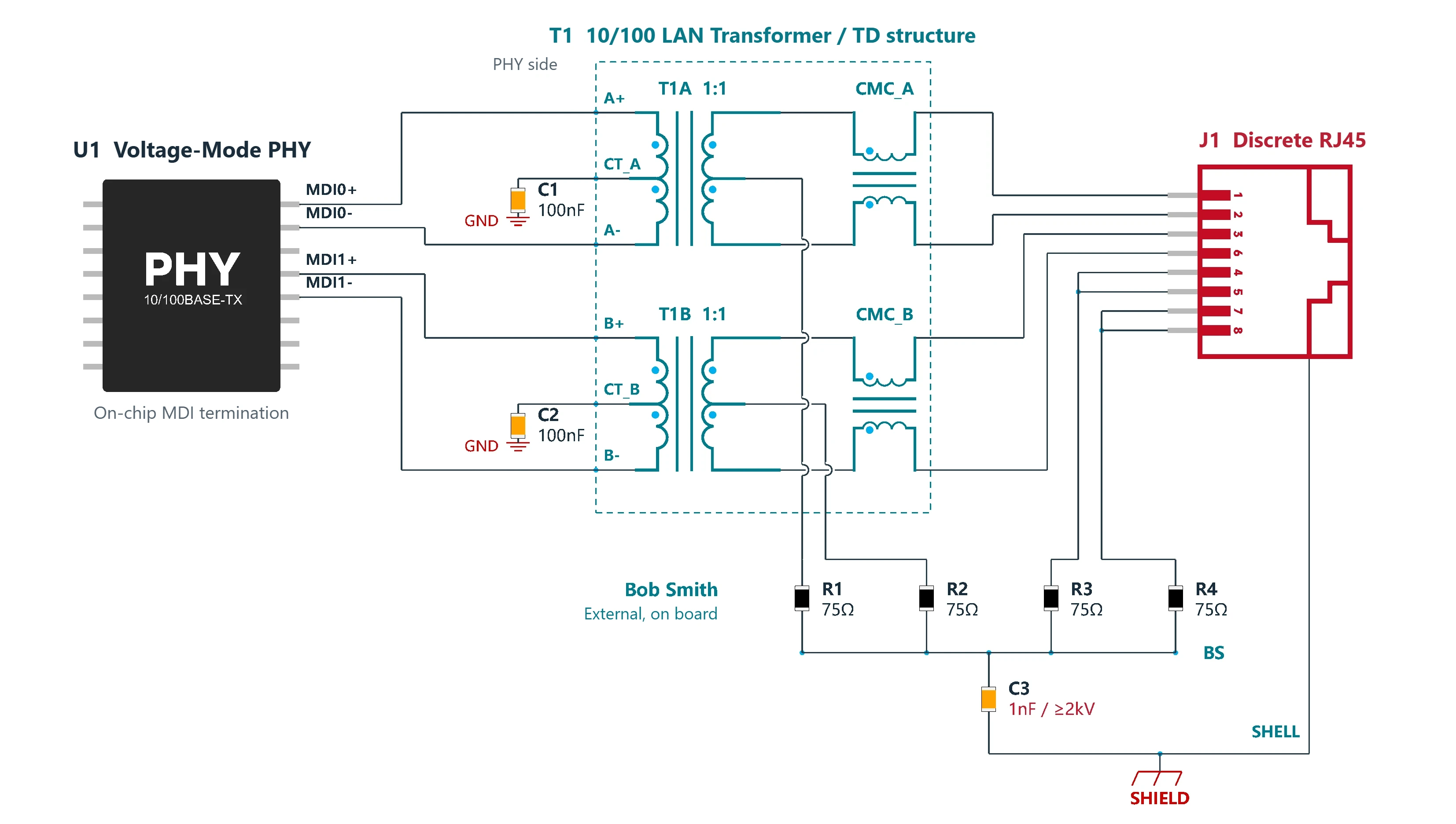
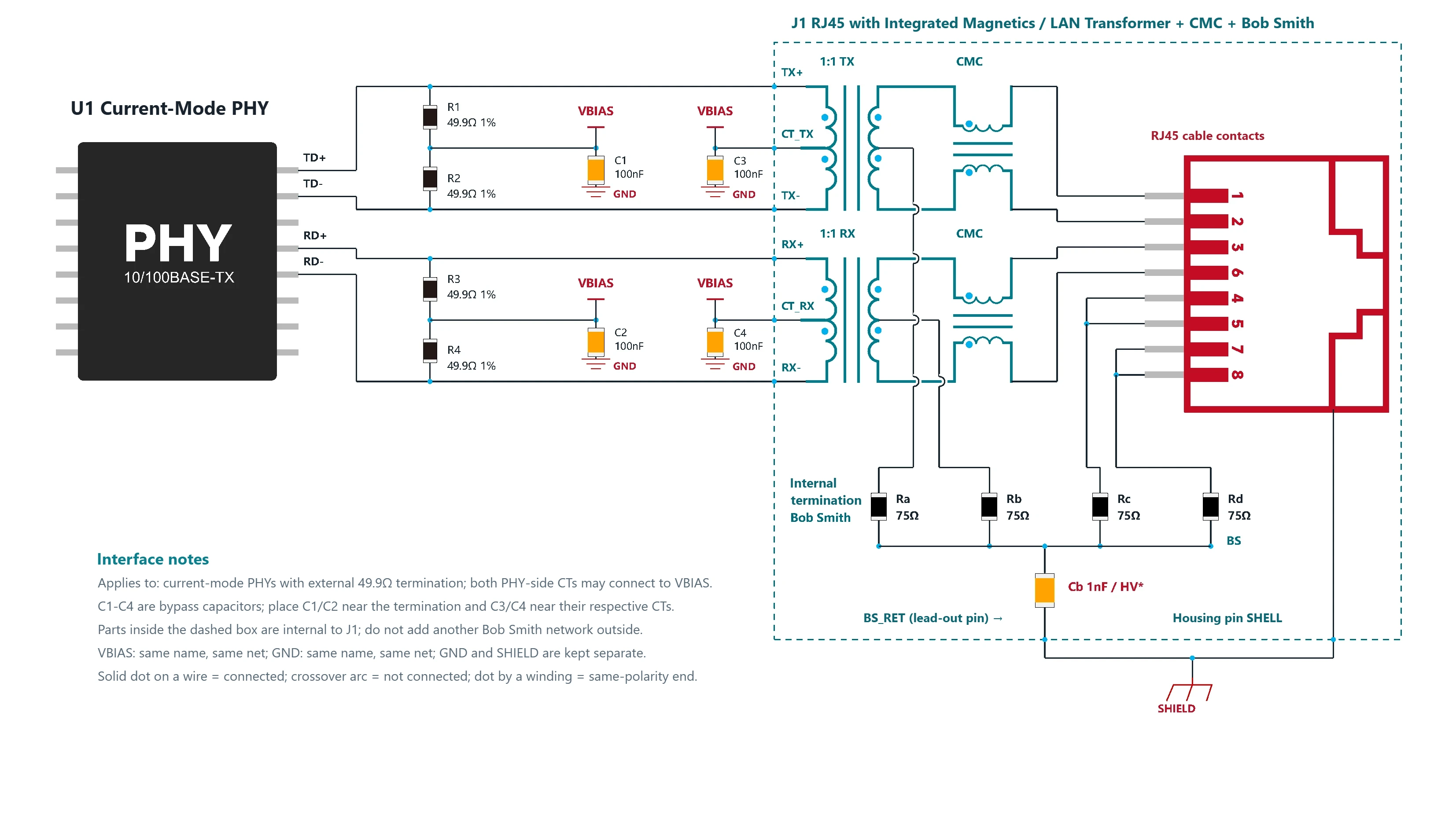
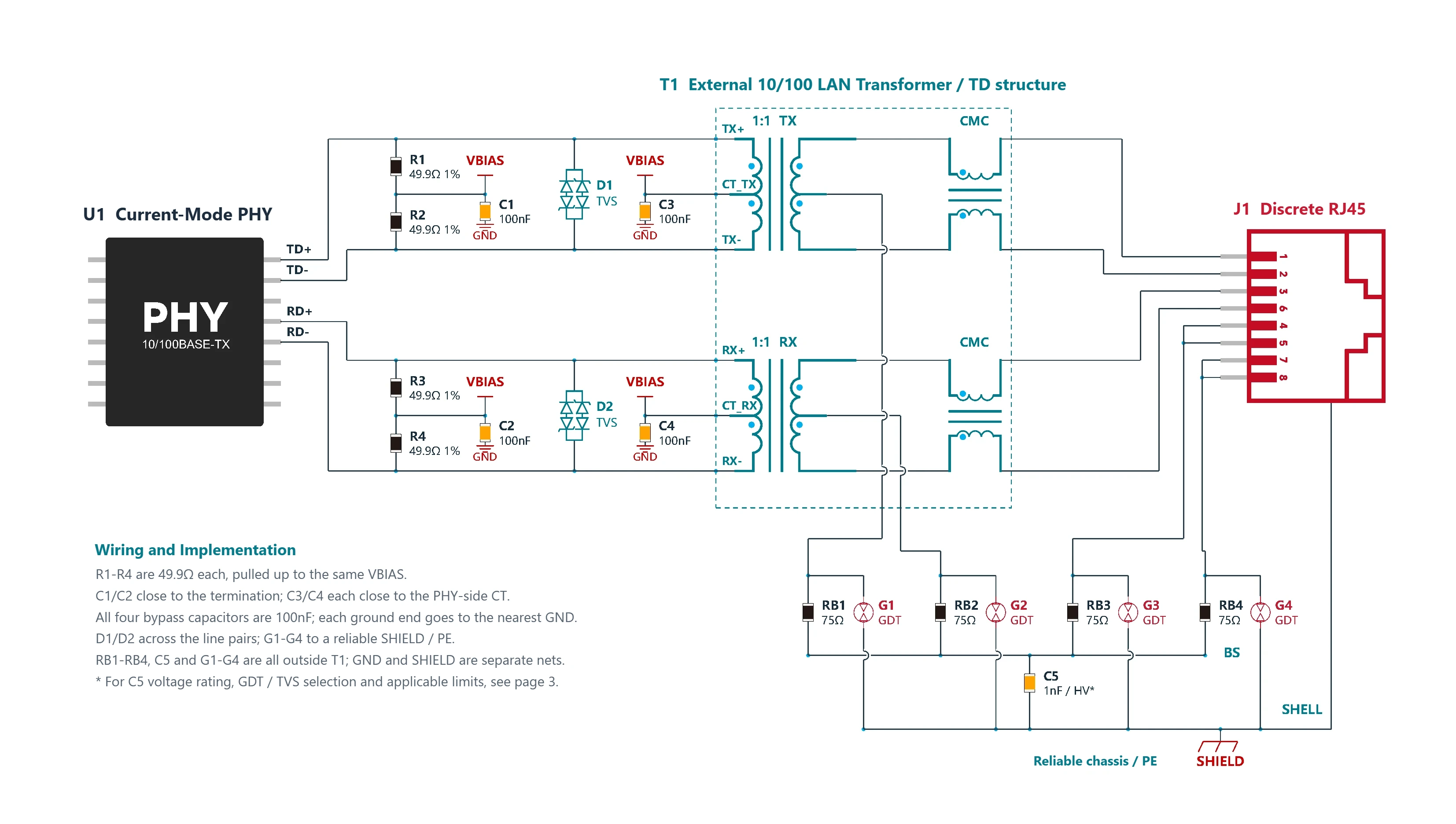
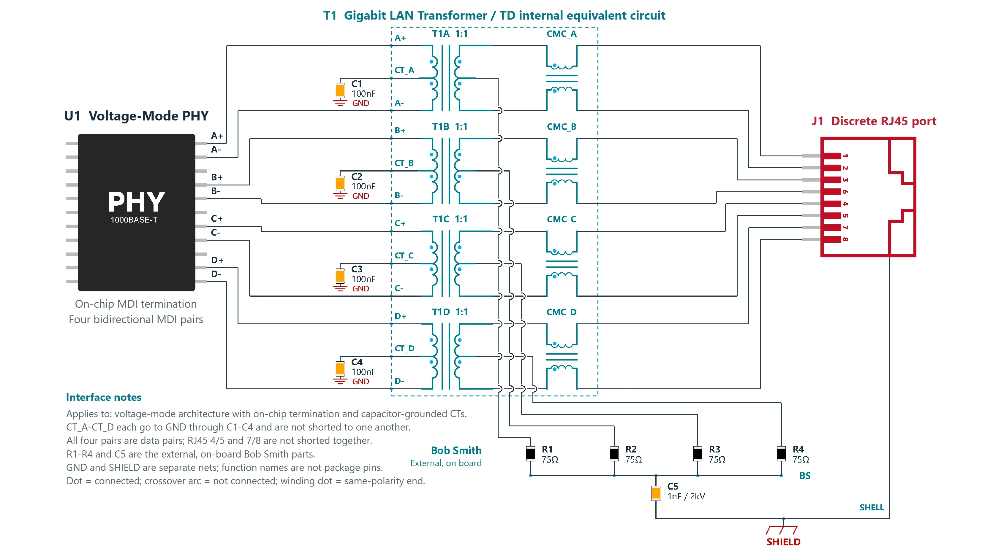
Transformerless Ethernet Port: 10/100BASE-TX Capacitive Coupling with Chip LAN Common-Mode Choke (Voltage-Mode PHY) · Standard reference design schematic (D1.1)
Key points: transformerless Ethernet port circuit
Design target and conditions of use
For non-PoE Ethernet ports that connect to an external network cable, with a target maximum cable length of 100 m. Uses a voltage-mode PHY that supports capacitive coupling and on-chip termination. This edition is a dedicated validation circuit: 100 m interoperability and full standards compliance are not yet confirmed.
Signal coupling and protection
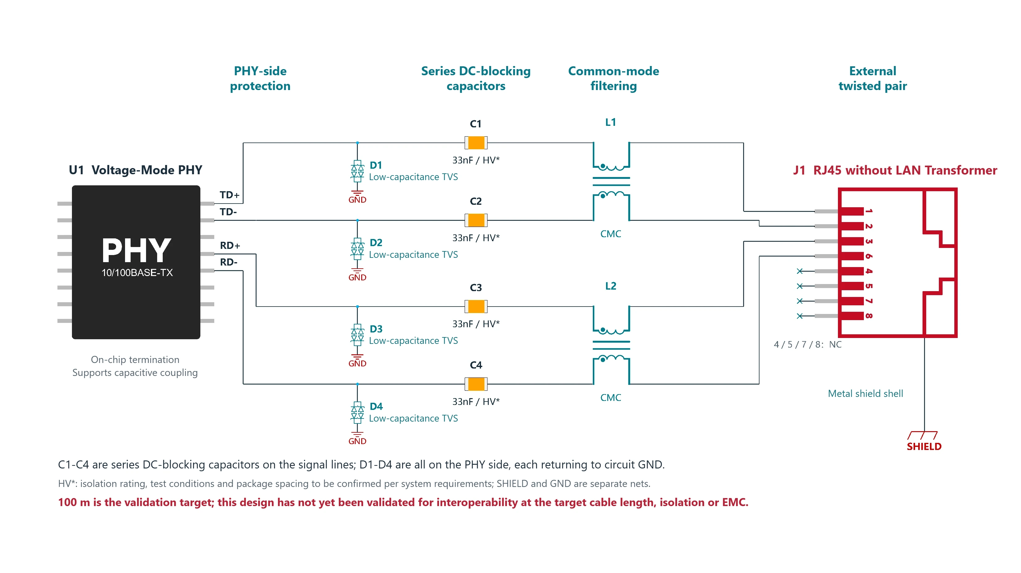
Each TD± and RD± line has one of C1–C4 in series (33 nF reference value) for DC-blocking coupling. D1–D4 each connect to GND on the PHY side of the capacitors; use low-capacitance TVS diodes matched to the PHY. These capacitors are not power-supply decoupling parts.
Common-mode filtering and RJ45 connection
L1 and L2 are in series with the two differential pairs, one per pair. In standard MDI, TX± connects to RJ45 cable contacts 1/2 and RX± to 3/6; contacts 4, 5, 7 and 8 are each NC. The schematic has no center-tap supply, no external 49.9Ω pull-ups and no Bob Smith network.
Grounding and isolation
The metal shell connects to SHIELD; circuit GND and SHIELD are separate nets. Select C1–C4 and the spacing across the isolation boundary based on port isolation testing; do not judge by the capacitors' nominal voltage rating alone. An autotransformer winding is not an isolation component and is not included in this schematic.
Layout requirements
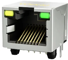
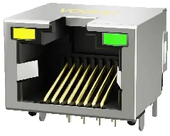
Design the MDI for 100Ω differential impedance, lay out each pair symmetrically, and keep the TVS ground return short. Complete the PHY power, clock, reset, MAC and LED circuits separately. Check how the parts shown in the product images fit this circuit during part selection.
How to read the schematic: transformerless Ethernet port
C1–C4 are series DC-blocking capacitors in the signal lines. D1–D4 are all on the PHY side, each returning to circuit GND.
HV*: Determine the isolation rating, test conditions and package spacing from the system requirements. SHIELD and GND are separate nets.
100 m is the validation target. Interoperability at the target cable length, isolation and EMC have not yet been validated for this schematic.
Functional pin names do not represent package pin numbers; the RJ45 numbers are cable contacts. A dot indicates a connection; a crossover arc indicates no connection. Do not short the NC pins to each other.
The part numbers above are the VOOHU parts listed under "Product images" in this reference design PDF, for selection reference. Check the final part numbers item by item against the PHY vendor documentation and the circuit parameters.
Need a quote or samples for these parts? Send your quantity and PHY model to a VOOHU FAE, who will check the part selection against this reference design.
Choose an implementation that supports capacitive coupling and on-chip termination. No CT supply and no external pull-up termination. The generic functional pins shown do not replace the package and register configuration of a specific part.
[1][2]; Architecture is conditional
C1–C4 / 33 nF / HV*
4; one in series per line
The vendor's DC-blocking value is used as the starting point for validation. Non-polarized and matched in pairs. Tolerance, dielectric, isolation rating, duration, leakage current and spacing must be determined during part selection. A DC voltage rating does not equal AC isolation capability; do not substitute ordinary low-voltage MLCCs.
Each MDI line has a TVS to circuit GND before its capacitor. The working voltage must cover the signal and common-mode range; the clamping voltage, dynamic resistance, junction capacitance and residual voltage must be coordinated with the PHY. The schematic shows a functional equivalent; the part number and protection level are not defined.
[2] Figure 39; [3] Protection
L1 / L2 / two-line CMC
2; between the capacitors and the RJ45
Provide common-mode filtering for the two pairs. Select for an impedance curve, insertion loss, return loss and balance suited to 10/100M. They are not series differential-mode inductors, and must not be selected by the 2012 package alone.
[2][3]; Placement is this edition's engineering implementation
J1 / SHIELD / RJ45 without magnetics
1; cable side
The pairs are on 1/2 and 3/6; each of the other contacts is left open. The shell connects to SHIELD; GND is a separate net. This edition does not add unvalidated unused-pair termination or GND-SHIELD coupling.
[2] Figure 39; Functional pin mapping
Autotransformer / not fitted in this schematic
0
For this edition, no vendor connection method matching the selected capacitive-coupling architecture was found. An autotransformer winding cannot provide primary-to-secondary isolation; connecting its tap directly to GND would create a DC path from the cable to circuit ground.
[1][2] Inferred from the connectivity of the main figures
100 m target / pending dedicated validation
Entire link; not a component rating
The vendors' existing long-cable tests cannot be generalized across PHYs, link partners or environments. Validate 10M/100M operation, auto-negotiation and MDI-X, long and short cables, link drops / bit errors, transmit waveforms and return loss, and complete isolation and EMC testing separately.
[2][3][4]; Not tested
Vendor documentation and scope of use
[1] · TI DP83826 datasheet, SNLS647I, 2025-08, p1, pp. 95–97, Figure 9-3. Basis: voltage-mode MDI and the four-line 33 nF DC-blocking structure. It is not used to claim that this schematic passes 100 m or EMC.
[2] · ADI ADIN1200 Rev.B, pp. 42–43, Figure 39; pp. 75–76, Table 98. Basis: on-chip termination, PHY-side TVS, CMC recommendation and short-cable range. For capacitive coupling with this device, the receive zero-power termination must be disabled.
[3] · ADI ADIN1300 and ADIN1200 with Capacitive Coupling, 2021-02-11, Protection / Configurations / Evaluation. The long-cable results are an example of ADIN1300 with capacitive coupling at both ends under nominal conditions; they do not replace validation of a general-purpose 10/100 Mbps port against ordinary link partners.
[4] · TI TLK110 Ethernet PHY Transformerless Operation, SLLA327, 2012-09, p3, pp. 6–8. The 120 m result applies only to the specific TLK110 circuit in that document, and the document states that it is not fully IEEE compliant. This schematic does not use its pull-up termination.
Limits of use
The main schematic is a prototype candidate circuit based on the vendors' capacitive-coupling architecture. 100 m is a user target; the part numbers, link partners and system test conditions are not yet closed, so this design cannot be described as meeting the requirements of an ordinary 100 m Ethernet port. Conditions to confirm before mass production: fix the actual PHY, CMC, TVS, DC-blocking capacitor and RJ45 part numbers; validate 0.5/1/10/50/100 m links and common magnetically coupled link partners at temperature and supply corners. For isolation testing, specify the test nodes, AC or DC, amplitude and duration; for EMC, specify the levels, coupling methods and pass criteria. If the design must directly meet the target of an ordinary 100 m Ethernet port, prefer a magnetically isolated architecture backed by corresponding validation evidence. This edition is for part selection and prototype validation; 100 m interoperability, port isolation and EMC have not been validated, and it is not a final design for mass production. The schematic, text and connection data have been reviewed; native EDA ERC, 100 m prototype testing, and isolation or EMC certification have not been performed.
FAQ: transformerless Ethernet port
Can a 10/100 Mbps Ethernet port skip the LAN transformer and use capacitive coupling directly?
Yes, under certain conditions, but this edition is a dedicated validation circuit. The PHY must be a voltage-mode PHY that supports capacitive coupling and on-chip termination, and each TD± and RD± line has one 33nF DC-blocking capacitor in series (the TI DP83826 vendor value, used as the starting point for validation). 100m interoperability and standards compliance are not yet confirmed. If the port must meet ordinary 100m Ethernet port requirements, prefer a magnetically isolated architecture backed by validation evidence.
Can ordinary low-voltage MLCCs be used as the DC-blocking capacitors?
No. C1–C4 are series DC-blocking capacitors in the signal lines, not power-supply decoupling parts, and a DC voltage rating does not equal AC isolation capability. They must be non-polarized and matched in pairs. Tolerance, dielectric, isolation rating, duration, leakage current and spacing across the isolation boundary must all be determined from port isolation testing during part selection; do not judge by the capacitors' nominal voltage rating alone.
In a capacitive-coupling design, which side of the capacitor does the TVS go on?
On the PHY side of the capacitor. For D1–D4, each MDI line has one low-capacitance bidirectional TVS to circuit GND before its DC-blocking capacitor, with a short ground return. The working voltage must cover the signal and common-mode range, and the clamping voltage, dynamic resistance, junction capacitance and residual voltage must be coordinated with the PHY. The schematic shows a functional equivalent; the part number and protection level are not defined.
Without a LAN transformer, are a center tap and Bob Smith termination still needed? Can an autotransformer be added?
Neither is used. This schematic has no center-tap supply, no external 49.9Ω pull-ups and no Bob Smith network. Contacts 4, 5, 7 and 8 are each NC, and the metal shell connects to SHIELD, which is a separate net from GND. No autotransformer is fitted in this schematic: it cannot provide primary-to-secondary isolation, and connecting its tap directly to GND would create a DC path from the cable to circuit ground.
Should the chip LAN common-mode choke be a 2012 or a 3216 package?
Do not select by package alone. L1/L2 are two-line CMCs in series between the capacitors and the RJ45. They provide common-mode filtering for the two pairs and are not series differential-mode inductors. Select them by an impedance curve, insertion loss, return loss and balance suited to 10/100M. During part selection, check how the WHLC-2012A and WHLC-3216A series shown in the product images fit this specific circuit.
Hello! Thank you for using the VOOHU official platform
To provide you with more accurate technical support, please fill in the following information
*We promise to strictly keep your information confidential, only for material delivery and follow-up technical support
Submission Successful
Thank you for your trust and support. Our engineering team will contact you within 1 business day to provide product selection recommendations and technical support
Talk to VOOHUWeekdays 8:30–18:00 (UTC+8) · first reply within 1 business day
Keep the site secure and working, and remember your language and cookie choice.
VOOHU
02
Analytics
Show us which pages are visited and how the site performs, so we can improve it.
Google Analytics · Ahrefs · VOOHU
03
Ad measurement
Measure which of our campaigns bring visitors to VOOHU.
Google Ads
04
Ad personalization
Show you more relevant VOOHU ads on other websites.
Google Ads · Meta · LinkedIn
In the EEA, the UK and Switzerland, analytics and advertising stay off until you allow them. Elsewhere, Google Analytics and Google Ads measurement are on by default, and ad personalization stays off until you allow it.
Changes save automatically
Privacy
Your privacy, your choice
We use cookies to run this site, understand how it’s used and measure our campaigns. Choose what’s on, and change it anytime in Cookie settings. Cookie Policy
✓Preferences saved. Change them anytime under Cookie settings in the footer.
WhatsApp Chat
Typically replies in minutes
Support
Hi! Thank you for connecting with VOOHU! How can we help you today?
Online now
We’ll open WhatsApp (mobile app or WhatsApp Web) with your message pre-filled.


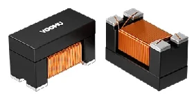 Chip LAN two-line common-mode choke (CMC)WHLC-3216A seriesMore signal line common-mode chokes →
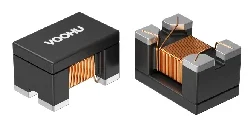 Chip LAN two-line common-mode choke (CMC)WHLC-2012A seriesMore signal line common-mode chokes →