Ethernet Port Surge Protection Circuit: 10/100BASE-TX ESD and Surge Reference Design (Current-Mode PHY) · Standard reference design schematic (D1.0)
Key design points of the Ethernet port surge protection circuit
Scope
Non-PoE 10BASE-T/100BASE-TX ports with a discrete RJ45 + external TD LAN transformer and a reliable chassis ground/PE. Applies to current-mode architectures with external 49.9Ω termination on each line and both PHY-side CTs connected to the bias supply.
Termination, bias and bypassing
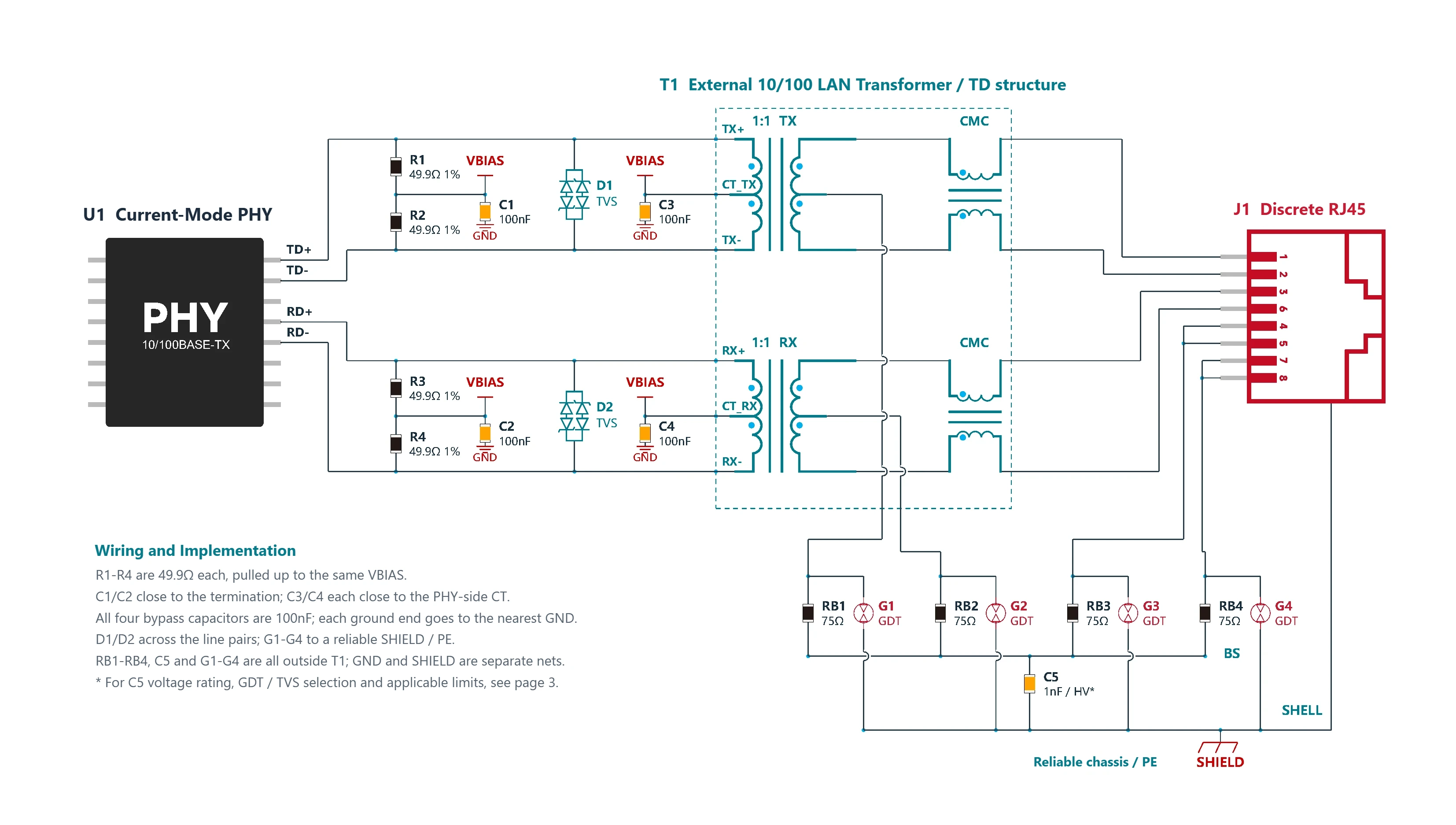
R1–R4 are 49.9Ω±1% each; each MDI signal connects to VBIAS through a resistor. C1/C2 are 100nF each, close to the termination. CT_TX/CT_RX also connect to VBIAS; C3/C4, 100nF each, connect to GND close by. Set the VBIAS value according to the PHY.
Magnetics and cable connections
T1 contains two 1:1 isolation transformers and cable-side CMCs. In standard MDI, TX± connects to RJ45 contacts 1/2 and RX± to 3/6; the unused contacts 4/5 and 7/8 are each tied together as a pair. Swapping the TX and RX pairs requires PHY support.
Staged protection
D1/D2 are PHY-side low-capacitance bidirectional differential-mode TVS diodes. G1/G2 connect from the cable-side CTs to SHIELD; G3/G4 connect from the two unused pairs to SHIELD. All of these connection points are before the 75Ω resistors. SHIELD connects to a reliable chassis/PE.
Common-mode termination and grounding
Each of the four branches joins BS through 75Ω, and BS connects to SHIELD through C5 (a 1nF high-voltage capacitor); the metal shell connects to the same net. GND and SHIELD are separate nets. Select the TVS, GDT, magnetics and C5 together to meet the protection and insulation targets; see page 3 for the basis.
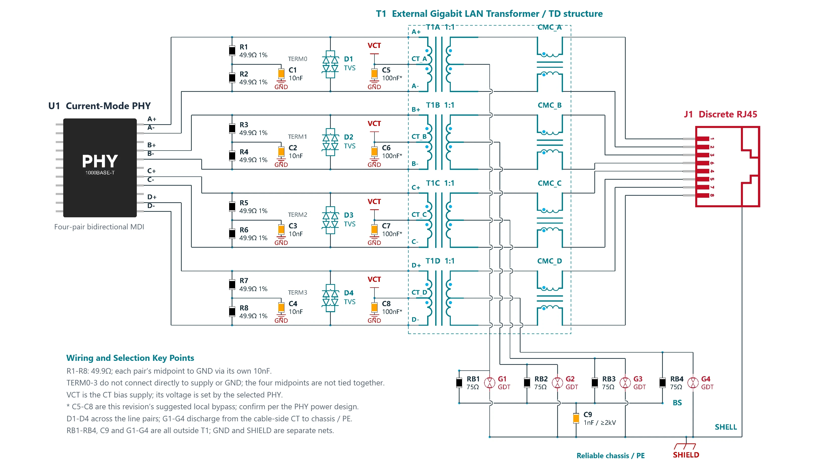
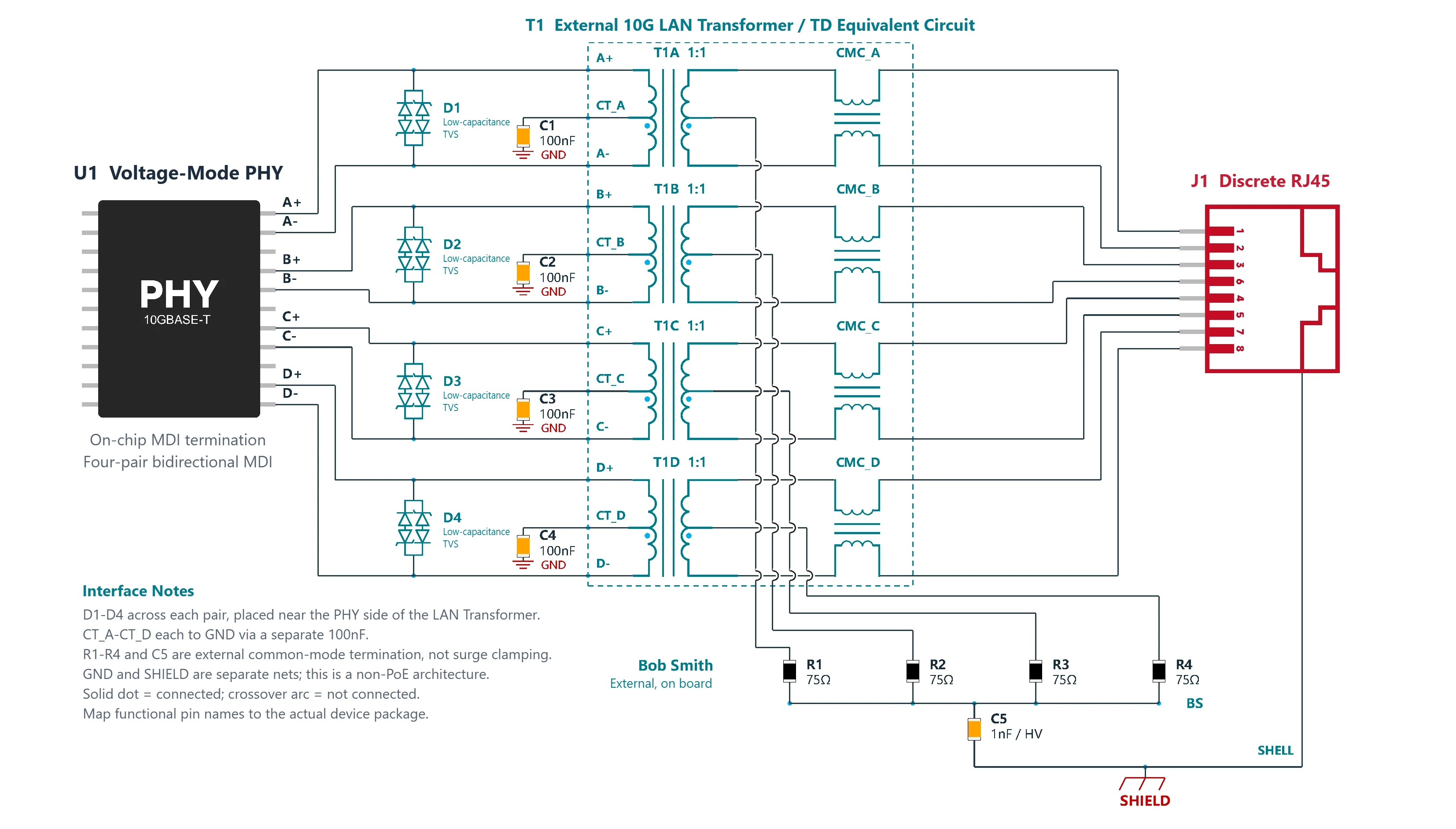
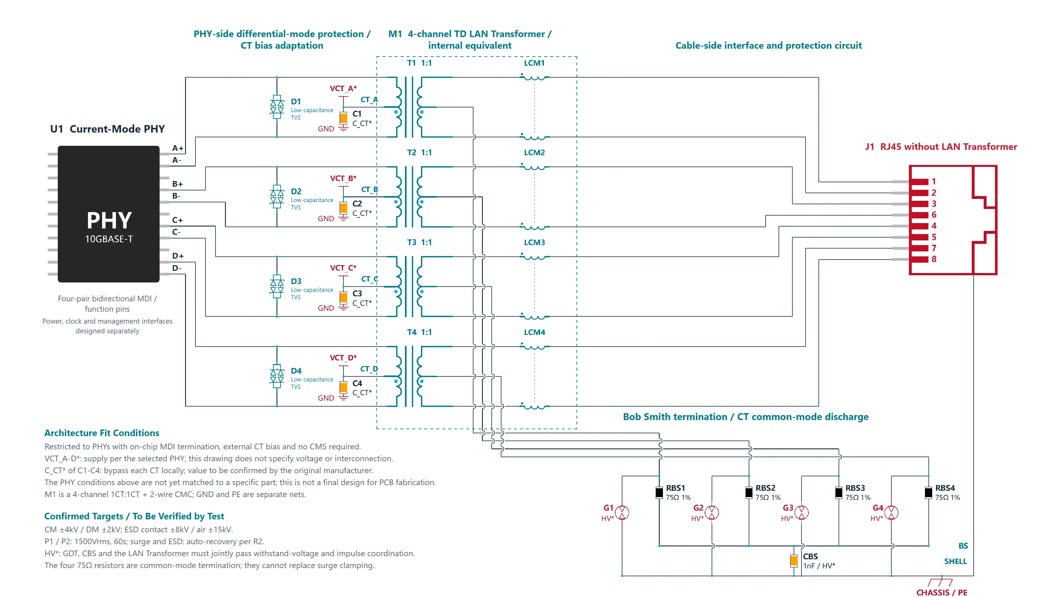
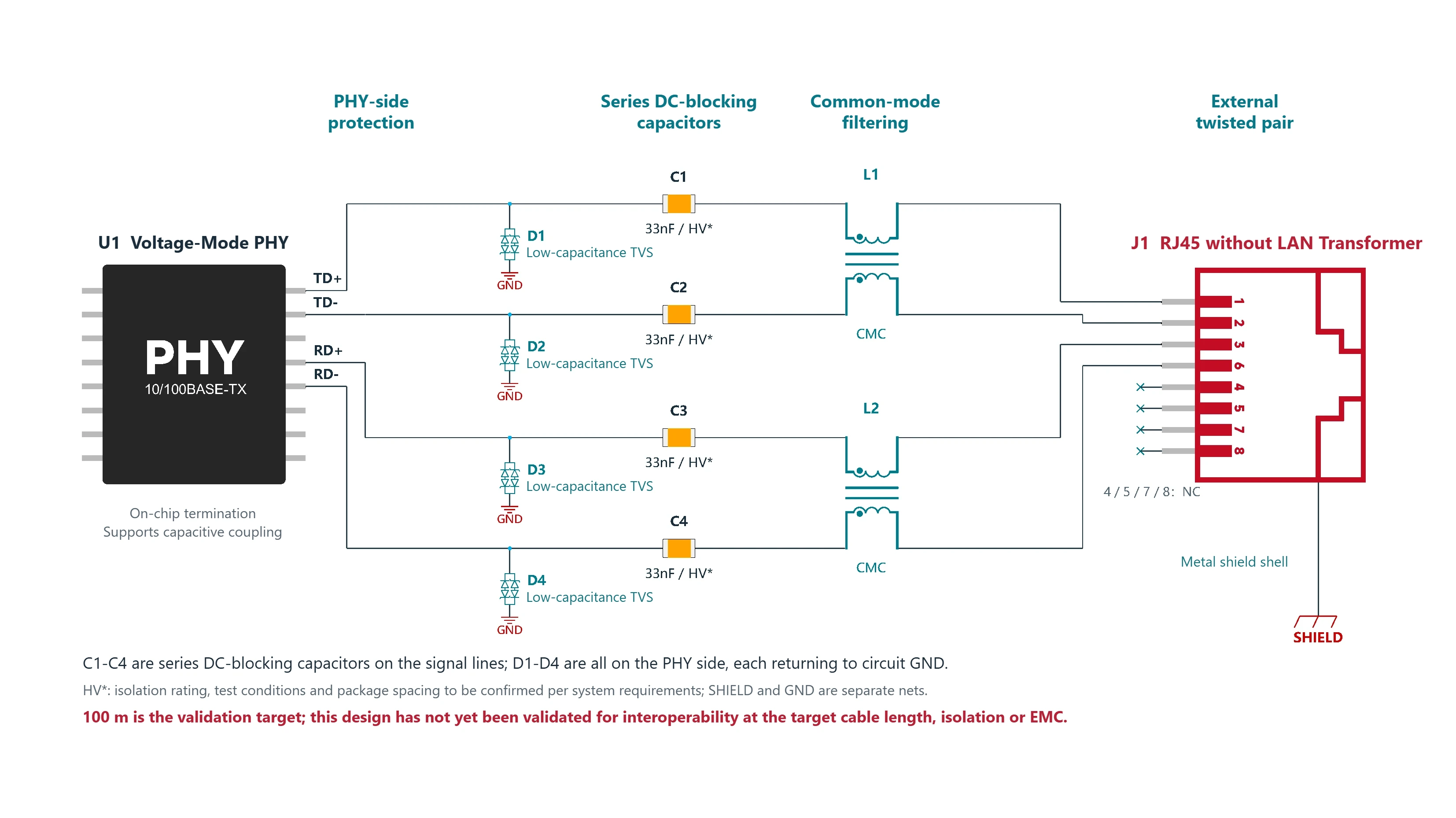
How to read the Ethernet port surge protection schematic
R1–R4 are 49.9Ω each, pulled up to the same VBIAS.
C1/C2 sit close to the termination; C3/C4 sit close to their respective PHY-side CTs.
All four bypass capacitors are 100nF; each ground end connects to GND close by.
D1/D2 are connected across the line pairs; G1–G4 connect to a reliable SHIELD / PE.
RB1–RB4, C5 and G1–G4 are all outside T1; GND and SHIELD are separate nets.
* See page 3 for the C5 voltage rating, GDT / TVS selection and limits of use.
Function terminal names are not package pin numbers; the RJ45 numbers are cable contacts. A solid dot marks a connection, a dot beside a winding marks the dotted (same-polarity) terminal, and a crossover arc means no connection. See page 3 for protection parameter selection.
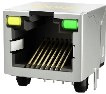
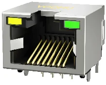
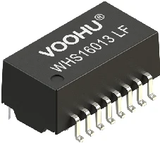
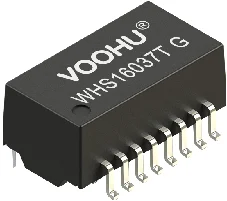
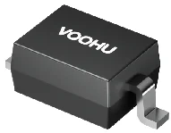
The part numbers above are the VOOHU parts listed under "Product illustrations" in this reference design PDF, provided for selection reference. Verify the final part numbers item by item against the PHY vendor documentation and the circuit parameters.
Need a quote or samples for these parts? Send your quantity and PHY model to a VOOHU FAE to check the part selection against this reference design.
Each TD±/RD± line connects to VBIAS through 49.9Ω±1%, giving about 100Ω differential termination. This applies only to this external-termination architecture. If the PHY has on-chip termination or different CT rules, redesign per its vendor documentation; do not reuse this circuit just because the PHY is "current-mode".
E1 Figure 3-4; E2 §2.1
C1–C4 / VBIAS
Four 100nF
C1/C2 sit beside the two termination pairs and C3/C4 beside their respective PHY-side CTs; all of them bypass VBIAS to GND. Even though VBIAS is a single net, each capacitor must still be placed close by. The DP83848 example uses 3.3V; the generic schematic does not fix the voltage.
E1 p. 4; E2 Figure 2
T1 / CMC
2 channels; TD structure
1:1 isolation transformer + cable-side common-mode choke; keep the polarity matched. Confirm the inductance, insertion loss, return loss, balance and insulation of the magnetics against the selected PHY. The GDT current path passes through the windings/CMC, so check their pulse withstand capability.
Basic interface: E2; Pulse check: E5
D1 / D2
2 differential-mode protection channels
Bidirectional low-capacitance TVS diodes across the PHY-side P/N, placed close to the LAN transformer with short branches. VRWM covers the normal differential swing; clamping, response and energy at the actual surge current must stay within the PHY's transient withstand. This branch does not directly clamp the pair's common-mode voltage.
E3 Figure 4; E5 pp. 6–9
G1–G4 / GDT
4 paths; outside T1
G1/G2: cable-side CT → SHIELD; G3/G4: unused pairs → SHIELD; all before the 75Ω resistors. When selecting, check impulse sparkover, surge current capacity, residual voltage and the port-to-chassis insulation test. This connection does not guarantee that the magnetics are protected from differential-mode surges.
CT local approach: E4 p. 8; Unused-pair extension: engineering design
RB1–RB4 / C5
4×75Ω + 1nF
The two CTs and the two unused pairs each join BS through 75Ω, and BS connects to SHIELD through C5. This forms the common-mode termination and does not replace the TVS/GDT. HV*: reference rating ≥2kV; confirm the AC/DC rating and pulse capability against the actual insulation requirement. Also check the pulse stress on the 75Ω resistors.
E2 pp. 4, 6; Part stress check: E5
J1 / shield / ground
1 discrete RJ45
TX to 1/2, RX to 3/6; in non-PoE use, 4/5 and 7/8 each form one group. SHELL, the GDTs and C5 return to a reliable chassis/PE; GND stays separate. Add the connector solder tabs, LEDs and the PHY power, clock and reset circuits according to the selected parts.
E2 §2.3–2.4; Grounding conditions to be confirmed by the user
Vendor documentation and scope of use
E1 · Texas Instruments SDAA089, 2025-09, p. 4 §3.2 / Figure 3-4. DP83848 10/100 Mbps current-mode example: 49.9Ω from each line to AVDD33, with 100nF close to the termination and to each CT. Used only for the architecture defined in this schematic; the bias in that example is 3.3V.
E2 · Texas Instruments AN-1469 / SNLA079D, 2013-04, pp. 4–7. Figure 2 and §2.1–2.4: magnetics, routing, common-mode termination and shielding. C5 follows the 1000pF and ≥2kV recommendation in the body text on p. 6; Figure 2 shows 1500pF, which is not treated as the only mandatory value.
E3 · Semtech Ethernet Protection Methodology, 2020-02-19, Figure 4. Adopts the approach of a TVS across each pair on the PHY side; choose the clamping and energy ratings based on the signal, the PHY's withstand and the actual pulse. The example test results in that document are not carried over as ratings for this design.
E4 · Littelfuse General Port Protection, 2024, pp. 8, 10. p. 8 is a PoE++ CT-to-ground protection example; only its local GDT discharge approach is adopted. p. 10 is an Ethernet staged protection example. Porting this to the present non-PoE circuit and extending it to the unused pairs is an engineering combination.
E5 · Bourns Ethernet and PoE Protection Technical Article, 2006-12, pp. 6–9. GDT firing can increase pulse stress on the PHY side, so check the coordination of the TVS and magnetics. Only the part-coordination principle is adopted; its historical test standards and ratings are not carried over.
Limits of use
This schematic uses TI's 10/100 Mbps current-mode interface example combined with TVS and GDT protection. The design rationale table separates the vendor-documented basis from engineering design. The protection parts and test conditions are not yet fixed, so there is no system-level protection rating for this combination yet. Layout and protection validation: design the MDI for 100Ω differential impedance; place R1–R4 and C1/C2 close to the PHY and C3/C4 close to the corresponding CTs; place D1/D2 close to the LAN transformer. Keep the GDT-to-PE return path short and wide, and keep it separate from the PHY area. After defining the IEC 61000-4-2/-4-5 level, waveform, coupling network, source impedance and pass criteria, verify the link, residual voltage, pulse stress and insulation. No fixed kV rating is promised. This design does not cover PoE, direct lightning strikes or sustained power-frequency faults. The products shown have not been confirmed as a match. The reference circuit is for design and part selection; final connections, part parameters and protection performance depend on the actual parts selected and on system-level validation results. This version has completed document, schematic and connection data review; no native EDA ERC, prototype protection testing or system certification has been performed.
Ethernet port surge protection FAQ
Should the 49.9Ω termination and center taps of a current-mode PHY connect to 3.3V?
Connect them to the same VBIAS, but VBIAS is not fixed at 3.3V. R1–R4 (49.9Ω±1% each) pull TD±/RD± up to VBIAS, CT_TX/CT_RX also connect to VBIAS, and C1–C4 (100nF each) bypass close by. 3.3V is only the value in the TI DP83848 example; set VBIAS according to the selected PHY. If the PHY has on-chip termination or different CT rules, redesign per its vendor documentation.
How should the unused pairs 4/5 and 7/8 be handled on a non-PoE 10/100 Mbps port?
Tie each pair together, then route it to BS through 75Ω. The two cable-side CTs and the two unused pairs each go through a series 75Ω resistor (RB1–RB4) to BS, and BS connects to SHIELD through C5 (a 1nF high-voltage capacitor). This forms the Bob Smith common-mode termination. G3/G4 connect from the unused pairs to SHIELD, before the 75Ω resistors. Adding GDTs on the unused pairs is an engineering design extension, not part of the vendor's original schematic.
What do the TVS and GDT each do? Which standards is Ethernet port surge protection tested to, and how many kV can it pass?
This design does not promise a fixed kV rating. D1/D2 are low-capacitance bidirectional differential-mode TVS diodes across P/N on the PHY side; they do not clamp the pair's common-mode voltage. G1–G4 discharge from the cable-side CTs and the unused pairs to SHIELD/PE. GDT firing can increase pulse stress on the PHY side, so check the coordination of the TVS and magnetics, and run system-level validation against the defined IEC 61000-4-2/-4-5 level and pass criteria.
What value and voltage rating should C5 in the Bob Smith circuit have?
The reference is 1nF rated ≥2kV, based on the 1000pF and ≥2kV recommendation in the body text on p. 6 of TI AN-1469; Figure 2 of that document shows 1500pF, which is not treated as the only mandatory value. Confirm the AC/DC rating and pulse capability of C5 against the actual insulation requirement, and check the pulse stress on the 75Ω resistors. C5 only forms the common-mode termination and cannot replace the TVS/GDT.
Hello! Thank you for using the VOOHU official platform
To provide you with more accurate technical support, please fill in the following information
*We promise to strictly keep your information confidential, only for material delivery and follow-up technical support
Submission Successful
Thank you for your trust and support. Our engineering team will contact you within 1 business day to provide product selection recommendations and technical support
Talk to VOOHUWeekdays 8:30–18:00 (UTC+8) · first reply within 1 business day
Keep the site secure and working, and remember your language and cookie choice.
VOOHU
02
Analytics
Show us which pages are visited and how the site performs, so we can improve it.
Google Analytics · Ahrefs · VOOHU
03
Ad measurement
Measure which of our campaigns bring visitors to VOOHU.
Google Ads
04
Ad personalization
Show you more relevant VOOHU ads on other websites.
Google Ads · Meta · LinkedIn
In the EEA, the UK and Switzerland, analytics and advertising stay off until you allow them. Elsewhere, Google Analytics and Google Ads measurement are on by default, and ad personalization stays off until you allow it.
Changes save automatically
Privacy
Your privacy, your choice
We use cookies to run this site, understand how it’s used and measure our campaigns. Choose what’s on, and change it anytime in Cookie settings. Cookie Policy
✓Preferences saved. Change them anytime under Cookie settings in the footer.
WhatsApp Chat
Typically replies in minutes
Support
Hi! Thank you for connecting with VOOHU! How can we help you today?
Online now
We’ll open WhatsApp (mobile app or WhatsApp Web) with your message pre-filled.