10/100BASE-TX Ethernet Schematic: Discrete RJ45 + External LAN Transformer (Voltage-Mode PHY) · Standard reference design schematic (D1.0)
10/100BASE-TX Ethernet port circuit: key design points
Scope
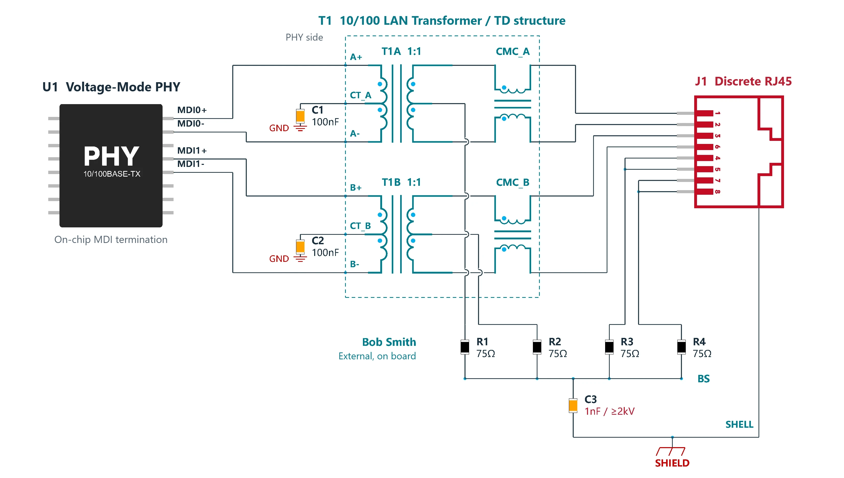
Non-PoE, discrete RJ45 + external 10/100 Mbps LAN transformer. For voltage-mode PHYs that use on-chip MDI termination and allow each of the two CTs to be grounded through its own capacitor.
PHY-side connections
Connect MDI0± to T1A and MDI1± to T1B. Do not add external 49.9Ω resistors on the data lines. Connect CT_A and CT_B to GND through C1 and C2 (100nF) respectively. Keep the two CTs separate, with no bias supply. Place each capacitor right next to its CT.
LAN transformer and cable connections
T1 is a TD structure: two 1:1 isolation transformers + cable-side CMCs. A± connects to RJ45 contacts 1/2 and B± to 3/6. Which pair transmits and which receives depends on the PHY's MDI/MDI-X configuration.
Bob Smith termination and shield
The two cable-side CTs connect to BS through R1 and R2 respectively. Contacts 4/5 are tied together, and so are 7/8; the two groups then connect to BS through R3 and R4 respectively. R1–R4 are all 75Ω. BS connects to SHIELD through C3 (1nF, rated voltage ≥2kV), and the metal shell connects directly to the same SHIELD.
Implementation limits
R1–R4 and C3 are all external parts on the board. GND and SHIELD are separate nets; how they relate at the system level is designed separately. Add the PHY power, clock, reset, MAC and LED circuitry for the actual parts used, and map the function names and contact numbers to the actual solder pins.
How to read the 10/100BASE-TX Ethernet port schematic
Function names are not package pin numbers. The RJ45 numbers are cable contacts.
A solid dot marks a connection. The dot next to a winding marks its dotted (same-polarity) terminal. An arc where two lines cross means they are not connected.
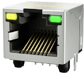
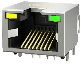
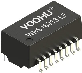
The part numbers above are the VOOHU parts listed under "Product illustrations" in this reference design PDF, for selection reference. Verify the final part numbers item by item against the PHY vendor documentation and the circuit parameters.
Need a quote or samples for these parts? Send the quantity and PHY model to a VOOHU FAE to check the selection against this reference design.
Uses a 10/100 Mbps architecture with on-chip MDI termination and PHY-side CTs grounded through capacitors, so no external 49.9Ω resistors or CT bias supply are added. The "voltage-mode" label alone does not determine the full peripheral circuit.
E1 p42; E2 p1
C1, C2 / 100nF
2, outside T1
C1 connects CT_A to GND and C2 connects CT_B to GND, giving the common-mode component an AC bypass while blocking DC. The two CTs are independent, each with its own capacitor placed right next to its pin. Choose the actual voltage rating, dielectric and package for the operating conditions.
Connection: E1 pp. 42–43; Close to CT: E3 p4
T1A, T1B / 1:1
2 channels, inside T1
Provide isolated coupling for the two differential pairs. Both sides have center taps. The part must meet the target PHY's inductance, insertion loss, return loss, common-mode and insulation requirements. The TD shown consists of an isolation transformer and a CMC, with no autotransformer stage.
E1 pp. 42–43, Table 28; E3 p4 Figure 2
CMC_A, CMC_B
2 channels, inside T1
Two-winding common-mode chokes in series in the cable-side data path attenuate common-mode noise. Keep the two windings and their dotted terminals paired so that each differential channel passes straight through. Do not short the two data lines together.
E1 p42; E3 p4, p7
R1–R4 / 75Ω
4, outside T1
R1/R2 connect to the two cable-side CTs; R3/R4 connect to the 4/5 and 7/8 pairs. Each path passes through its own 75Ω before joining BS. ±1% is the selection recommendation for this version. These resistors provide common-mode termination; they are not PHY-side differential termination.
E3 p4 Figure 2, p6 §2.3; Tolerance is an engineering recommendation
C3 / 1nF, ≥2kV
1, outside T1
BS connects to SHIELD through C3, which provides a high-frequency common-mode return path while blocking DC. The voltage rating follows the vendor's recommendation. For the actual part, check the AC/DC ratings, test conditions and insulation certification. This voltage rating does not represent the system surge rating.
E3 p6 §2.3
J1 / discrete RJ45
1
A± → 1/2, B± → 3/6. 4/5 form one group and 7/8 another; each group connects to BS through one 75Ω. This applies only to the non-PoE 10/100 Mbps use in this version. Map the RJ45 contact numbers to the solder pins of the actual connector. The metal shell connects to SHIELD.
E3 p4, pp. 6–7; Mapping per this schematic
GND / SHIELD
Two nets
GND connects the PHY-side capacitors; SHIELD connects the Bob Smith capacitor and the metal shell. The schematic adds no fixed RC network between GND and SHIELD. Their relationship to the chassis/PE and the coupling location follow the system's mechanical, insulation and EMC design.
E3 p7 §2.4; Coupling scheme to be decided at system level
Vendor documentation and scope of use
E1 · Analog Devices ADIN1200 datasheet, Rev.B, 2024-05. p24, Table 18; pp. 42–43, Magnetics, Figure 38, Table 28; pp. 86–87, PCB Layout. Used here: MDI mapping, on-chip termination and separate 100nF grounding. Figure 38 includes an autotransformer stage; this schematic uses two-stage TD magnetics instead.
E2 · Texas Instruments DP83825I datasheet, SNLS638C, 2026-04. p1, pp. 86–87 §8.4: 10/100 Mbps voltage-mode driver, on-chip MDI termination and 100Ω differential routing. Its power supply and package parameters are not used in the generic main schematic.
E3 · Texas Instruments AN-1469, SNLA079D, 2013-04. p4 Figure 2, p6 §2.3, p7 §2.4. Only the cable-side (post-isolation) termination and shielding principles are used. 1nF/≥2kV is taken from the p6 text; Figure 2 shows 1500pF instead. The PHY-side supply and the 49.9Ω resistors are not used.
Limits of use
This page is an MDI interface reference circuit. It does not cover the complete PHY peripheral circuitry and contains no protection certification conclusions. The reference circuit is for design and part selection; the final connections, part specifications and system performance depend on your actual selection and validation results. It is released for selection review after the documentation check and the schematic and text review were completed; no prototype, EDA ERC or system certification tests have been performed. Layout requirements: route the two MDI pairs at 100Ω differential impedance, short and symmetric, with as few stubs and layer changes as possible. Keep a continuous reference plane on the PHY side; determine the copper and spacing in the isolation area separately.
10/100BASE-TX Ethernet port circuit FAQ
Should the LAN transformer center taps of a voltage-mode PHY connect to 3.3V?
Not in this design. CT_A and CT_B each connect to GND through one 100nF capacitor. The two CTs stay separate and do not connect to a bias supply. This assumes the PHY uses on-chip MDI termination and allows its CTs to be grounded through capacitors. The "voltage-mode" label alone does not determine the full peripheral circuit; verify it against the documentation for the PHY you select.
How should the unused RJ45 pins (4/5, 7/8) on a 10/100 Mbps Ethernet port be handled?
Tie 4/5 together and 7/8 together, then connect the two groups to BS through R3 and R4 (75Ω) respectively. The two cable-side CTs also connect to BS, through R1 and R2 (75Ω) respectively. BS then connects to SHIELD through C3 (1nF, rated voltage ≥2kV). This connection applies only to the non-PoE 10/100 Mbps use in this version. Map the contact numbers to the solder pins of the actual connector.
Do the data lines need additional 49.9Ω termination resistors? What are the 75Ω resistors for?
No additional resistors are needed. The PHY in this design uses on-chip MDI termination, so no external 49.9Ω is added on the data lines. The 75Ω resistors R1–R4 are Bob Smith common-mode termination. They sit on the cable side of the LAN transformer and join at BS; they are not PHY-side differential termination. The ±1% tolerance is the selection recommendation for this version.
What is the TD structure in a LAN transformer, and which parameters should you check when selecting one?
TD means two 1:1 isolation transformers plus cable-side two-winding common-mode chokes (CMC); the version shown has no autotransformer stage. The part must meet the target PHY's inductance, insertion loss, return loss, common-mode and insulation requirements. Also check the complete pinout, the internal CT/CMC structure and the 10 Mbps mode specifications, then complete link, return loss and EMC validation.
C3 is marked 1nF/≥2kV. Does that mean the port can withstand a 2kV surge?
No. The ≥2kV voltage rating follows the recommendation in the TI AN-1469 text. C3 forms the high-frequency common-mode path from BS to SHIELD and blocks DC. For the actual part, check the AC/DC ratings, test conditions and insulation certification. This voltage rating does not represent the system surge rating, and this page contains no protection certification conclusions.
Hello! Thank you for using the VOOHU official platform
To provide you with more accurate technical support, please fill in the following information
*We promise to strictly keep your information confidential, only for material delivery and follow-up technical support
Submission Successful
Thank you for your trust and support. Our engineering team will contact you within 1 business day to provide product selection recommendations and technical support
Talk to VOOHUWeekdays 8:30–18:00 (UTC+8) · first reply within 1 business day
Keep the site secure and working, and remember your language and cookie choice.
VOOHU
02
Analytics
Show us which pages are visited and how the site performs, so we can improve it.
Google Analytics · Ahrefs · VOOHU
03
Ad measurement
Measure which of our campaigns bring visitors to VOOHU.
Google Ads
04
Ad personalization
Show you more relevant VOOHU ads on other websites.
Google Ads · Meta · LinkedIn
In the EEA, the UK and Switzerland, analytics and advertising stay off until you allow them. Elsewhere, Google Analytics and Google Ads measurement are on by default, and ad personalization stays off until you allow it.
Changes save automatically
Privacy
Your privacy, your choice
We use cookies to run this site, understand how it’s used and measure our campaigns. Choose what’s on, and change it anytime in Cookie settings. Cookie Policy
✓Preferences saved. Change them anytime under Cookie settings in the footer.
WhatsApp Chat
Typically replies in minutes
Support
Hi! Thank you for connecting with VOOHU! How can we help you today?
Online now
We’ll open WhatsApp (mobile app or WhatsApp Web) with your message pre-filled.


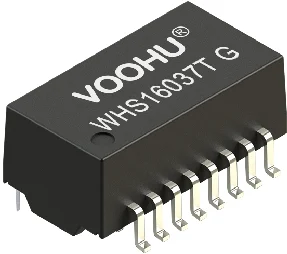 10/100 Mbps LAN transformer (TD, industrial grade)WHS16037TG (industrial grade)View WHS16037TG (industrial grade) →