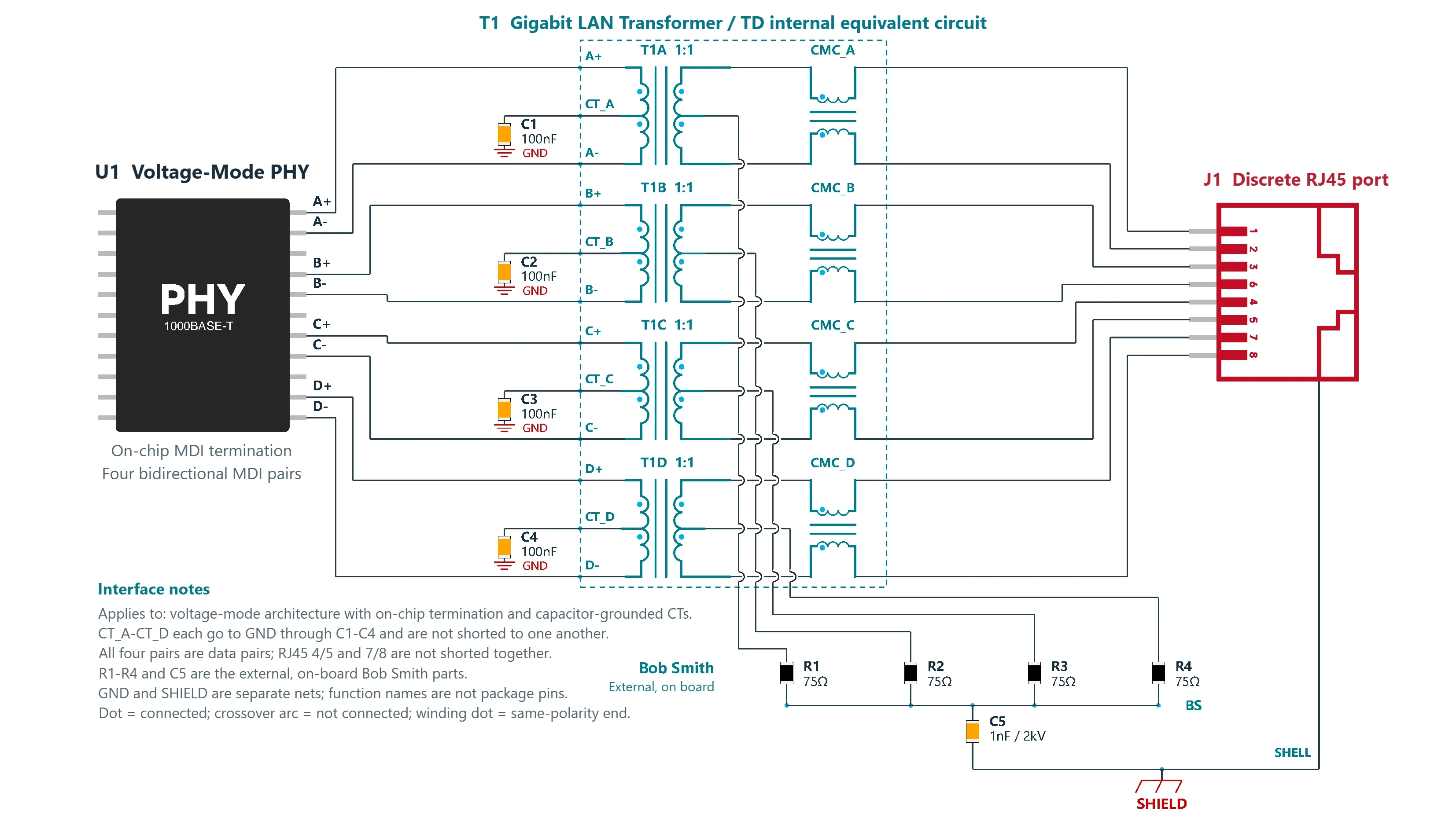
10GBASE-T Ethernet Surge and ESD Protection Circuit (Voltage-Mode PHY) · Standard reference design schematic (D1.0)
Key design points of the 10G Ethernet port surge protection circuit
PHY and center taps
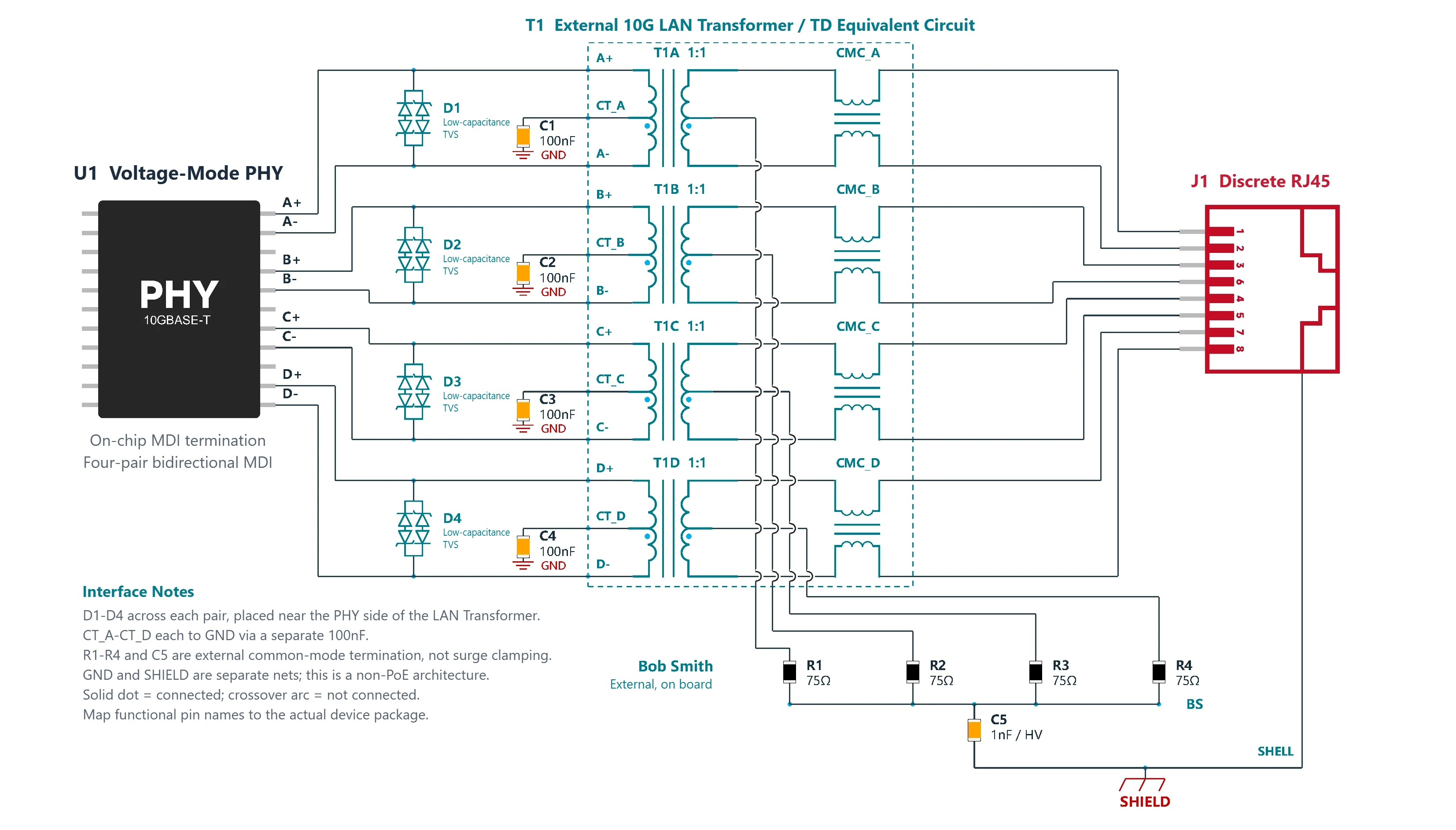
Uses a 10G voltage-mode PHY with on-chip termination; all four MDI pairs transmit and receive bidirectionally. CT_A–CT_D connect to GND through C1–C4 (100nF) respectively. The four paths are independent of each other, and each capacitor sits close to its LAN transformer pin. The CTs do not connect to an external bias supply.
LAN transformer and pair mapping
T1 uses a TD structure (four 1:1 isolation transformers plus cable-side CMCs) and must meet the 10G magnetics requirements of the selected PHY. Pairs A/B/C/D connect to RJ45 pins 1/2, 3/6, 4/5 and 7/8 respectively; all four are data pairs.
Surge and ESD clamping
D1–D4 are low-capacitance bidirectional TVS diodes, each connected across the positive and negative lines of one MDI pair. Place them near the LAN transformer on its PHY side, with connections as short as possible. They limit differential-mode transients coupled to the PHY side; their working voltage, clamping characteristics and parasitic capacitance must suit the actual PHY.
Common-mode termination and shield
Each cable-side CT goes through R1–R4 (75Ω) to the BS node, which connects to SHIELD through C5 (1nF high-voltage capacitor). The RJ45 metal shell connects to the same SHIELD. The Bob Smith network provides common-mode termination; it does not replace TVS clamping.
Scope
Non-PoE. Applies to architectures with on-chip termination and CTs grounded through capacitors. GND and SHIELD are separate nets. This schematic is a port protection reference for induced surge and ESD; the target levels and chassis grounding conditions are still to be determined. Complete the PHY's other supporting circuits according to the part selected.
How to read the 10G Ethernet port surge protection schematic
D1–D4: one across each pair, near the LAN transformer on its PHY side.
CT_A–CT_D each connect to GND through a separate 100nF.
R1–R4 and C5 are external common-mode termination, not surge clamping.
GND and SHIELD are separate nets; this schematic is a non-PoE architecture.
Solid dot = connected; crossover arc = not connected.
Map the functional pin names to the actual part package.
The part numbers above are the VOOHU parts listed under "Product images" in this reference design PDF, for selection reference. Verify the final part numbers item by item against the PHY vendor documentation and the circuit parameters.
Need a quote or samples for these parts? Send your quantity and PHY model to a VOOHU FAE to check the part selection against this reference design.
A 10G architecture with on-chip MDI termination, where the CTs need only capacitor decoupling. Do not add external 49.9Ω or 100Ω differential termination on top of it. Complete the power, clock, reset, management and MAC interface according to the actual PHY.
E1 pp. 59–60, p. 91; E2 drawing p. 12
C1–C4 / 100nF
4, outside T1
Each connects one of the four PHY-side CTs to GND, providing a common-mode AC return path. Place the capacitors close by; do not short the CTs together or connect them to an external supply. 100nF is the value for this reference architecture, taken directly from the vendor's 10G circuit.
E2 p. 12: C501, C502, C504, C505
D1–D4 / low-capacitance bidirectional TVS
4, PHY side
One bidirectional clamp is connected between the positive and negative lines of each pair; the schematic shows only the two-terminal clamping function. The working voltage must cover the normal line-to-line swing, and the clamping waveform must stay below the PHY's transient withstand limit. Check capacitance, residual voltage and pulse capability for the line-to-line connection.
E3 Figure 4; E4 10G application listing
T1A–T1D / 1:1
4 channels, inside T1
Carry the differential signals by magnetic coupling and provide electrical isolation. Use a 10G LAN transformer that meets this PHY's requirements, and check insertion loss, return loss, crosstalk, balance, OCL and insulation. A matching turns ratio alone does not make it compatible.
E1 pp. 59–60; E2 p. 12; E3
CMC_A–CMC_D
4 channels, inside T1
A two-winding CMC in series with the two cable-side data lines suppresses common-mode noise. Together with the isolation transformer it forms the TD structure; this schematic has no autotransformer winding. Include the parasitics of the magnetics and their package in the 10G signal integrity assessment.
E3 Figures 1 and 4; Verify against the selected magnetics
R1–R4 / 75Ω
4, external on the board
Each of the four cable-side CTs goes through its own 75Ω before they join at BS. The resistors are not in series with the main differential path. Check pulse load and voltage rating; steady-state power rating alone cannot show surge capability.
E3 Figures 1 and 2
C5 / 1nF, HV
1, external on the board
BS connects to SHIELD through a high-voltage capacitor, forming an AC common-mode return path and blocking DC. HV means a high-voltage part selected for the actual insulation and pulse tests; DC voltage rating, AC withstand voltage and surge rating are not interchangeable.
E3 Figures 1 and 2
J1 / GND / SHIELD
Discrete RJ45; two separate ground nets
A→1/2, B→3/6, C→4/5, D→7/8. The RJ45 has no magnetics; its shell and the return end of C5 connect to SHIELD, and C1–C4 connect to GND. How SHIELD connects to the chassis, and whether it connects to PE, is decided by the system's mechanical design.
E1 pp. 59–60; E3 Figures 1 and 4
Vendor documentation and scope of use
E1 · Aquantia / Marvell AQR113/C Family Datasheet, Rev.1.0.7 (2018-10), pp. 59–60 and §4.13 p. 91: 10G MDI, 1:1 LAN transformer and voltage-mode CT decoupling. The link is a public repost of a document attributed to the vendor; obtain the applicable revision for mass production.
E2 · NXP LS1046ARDB-PB, SPF-29142 Rev.C, p. 12: each of the AQR113C's four CTs goes to ground through 0.1µF, with no external termination on the MDI. Only the PHY-side connection is taken from it; that board's CMS and the internal network of its special connector are not carried over.
E3 · Semtech Ethernet Protection Methodology (2020-02-19), Figures 1–4: PHY-side across-pair clamping, common-mode termination and protection coordination. Its example result at 500V, 1.2/50µs, 42Ω cannot be taken directly as proof that this schematic passes, or that a higher level passes.
E4 · Semtech RClamp3361P: official documentation explicitly lists 2.5G/5G/10GbE. Working voltage ±3.3V, typical capacitance 0.2pF, 8/20µs peak current 7A; for selection reference only. A part's rating is not the port's rating.
Limits of use
Interface protection reference: match the TVS diodes and magnetics to the actual PHY and the target test conditions. This schematic does not claim any system-level surge or ESD compliance level. Layout and validation: route the MDI to a 100Ω differential target, keep the TVS branches short, control intra-pair skew, and check for discontinuities caused by pads, vias and the magnetics. Complete 10G link, return loss / insertion loss, EMC and insulation tests. IEC 61000-4-5 / -4-2 tests must specify the waveform, source impedance, coupling method, common/differential mode, polarity and number of pulses, and pass criteria. To be determined: surge/ESD targets and chassis/PE conditions. This version uses a basic architecture of LAN transformer isolation + across-pair TVS and has no GDT; higher-energy protection needs separate coordination. The product images reuse display material; their suitability for 10G and for protection still needs to be confirmed from the part documentation.
10G Ethernet port surge protection FAQ
Should the center taps of a 10G voltage-mode PHY connect to a power supply?
No, they do not connect to a supply. This schematic uses a 10G voltage-mode PHY with on-chip termination. CT_A–CT_D each connect to GND through a separate 100nF capacitor (C1–C4); the four are not shorted together, and each capacitor sits close to its LAN transformer pin. The 100nF value comes from the vendor's 10G circuit: on the NXP reference board, each of the AQR113C's four CTs goes to ground through 0.1µF.
Does a voltage-mode 10G PHY need external 49.9Ω termination on the MDI lines?
No. U1 uses on-chip MDI termination, so this schematic does not add external 49.9Ω or 100Ω differential termination; the vendor reference board likewise has no external termination on the MDI. Complete the power, clock, reset, management and MAC interface according to the actual PHY. If the selected PHY requires external termination or CT bias, this schematic does not apply.
Which side of the LAN transformer should the low-capacitance TVS diodes go on, and how are they connected?
On the PHY side of the LAN transformer, connected across the positive and negative MDI lines of each pair (D1–D4, one bidirectional part per pair), with connections as short as possible. They limit differential-mode transients coupled to the PHY side. The working voltage must cover the normal line-to-line swing and the clamping waveform must stay below the PHY's transient withstand limit; check capacitance, residual voltage and pulse capability for the line-to-line connection.
With Bob Smith common-mode termination already in place, are TVS diodes still needed? Does this version have a GDT?
Yes, TVS diodes are still needed. R1–R4 (75Ω) and C5 (1nF high-voltage capacitor) form the external Bob Smith common-mode termination, which does not replace TVS clamping. This version uses a basic architecture of LAN transformer isolation + across-pair TVS and has no GDT (gas discharge tube); higher-energy protection needs a separately coordinated design.
How many kV of surge and ESD will a design built from this reference design pass?
This schematic does not claim any system-level surge or ESD compliance level; the target levels and chassis/PE grounding conditions are still to be determined. The example result in the Semtech document (500V, 1.2/50µs, 42Ω) cannot be taken as proof that this schematic passes. You must complete 10G link, return loss / insertion loss, EMC and insulation tests, plus IEC 61000-4-5/-4-2 tests under clearly defined conditions.
Hello! Thank you for using the VOOHU official platform
To provide you with more accurate technical support, please fill in the following information
*We promise to strictly keep your information confidential, only for material delivery and follow-up technical support
Submission Successful
Thank you for your trust and support. Our engineering team will contact you within 1 business day to provide product selection recommendations and technical support
Talk to VOOHUWeekdays 8:30–18:00 (UTC+8) · first reply within 1 business day
Keep the site secure and working, and remember your language and cookie choice.
VOOHU
02
Analytics
Show us which pages are visited and how the site performs, so we can improve it.
Google Analytics · Ahrefs · VOOHU
03
Ad measurement
Measure which of our campaigns bring visitors to VOOHU.
Google Ads
04
Ad personalization
Show you more relevant VOOHU ads on other websites.
Google Ads · Meta · LinkedIn
In the EEA, the UK and Switzerland, analytics and advertising stay off until you allow them. Elsewhere, Google Analytics and Google Ads measurement are on by default, and ad personalization stays off until you allow it.
Changes save automatically
Privacy
Your privacy, your choice
We use cookies to run this site, understand how it’s used and measure our campaigns. Choose what’s on, and change it anytime in Cookie settings. Cookie Policy
✓Preferences saved. Change them anytime under Cookie settings in the footer.
WhatsApp Chat
Typically replies in minutes
Support
Hi! Thank you for connecting with VOOHU! How can we help you today?
Online now
We’ll open WhatsApp (mobile app or WhatsApp Web) with your message pre-filled.


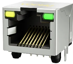
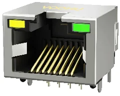
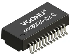
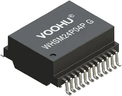 External 10G LAN transformer (for T1, TD structure)WHSM24P04PGMore LAN transformers →
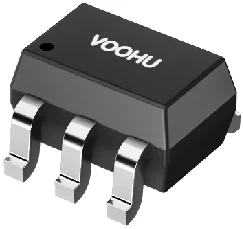
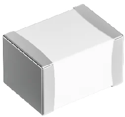 GDT gas discharge tube (display item only; this version's main schematic has no GDT)WHGD200V1P0BView WHGD200V1P0B →